ferroelectric composite cu 2 oVisible light photolysis of water to produce hydrogen photocathode and its preparation method
A technology of photolysis of water to produce hydrogen and visible light, which is applied in the field of photoelectrochemistry, can solve the problems of poor photocathode stability, photogenerated carrier separation and low transport efficiency, and achieve improved stability, improved life, and improved stability. Effect
- Summary
- Abstract
- Description
- Claims
- Application Information
AI Technical Summary
Problems solved by technology
Method used
Image
Examples
preparation example Construction
[0051] Ferroelectric Composite Cu 2 A preparation method of a photocathode for producing hydrogen by visible light photolysis of water, comprising the following steps:
[0052] Step 1. Place the silicon wafer substrate 1 on the deposition table in the vacuum chamber of the magnetron sputtering apparatus, with the Pt side of the silicon wafer substrate 1 facing up, and the air pressure in the vacuum chamber is 1×10 -4 -3×10 -4 Pa;
[0053] Step 2: Introduce a mixed gas of oxygen and argon with a volume ratio of 1:5-1:6 into the vacuum chamber of step 1, and control the air pressure in the vacuum chamber at 0.75-1Pa;
[0054] Step 3. Adjust the heating power of the magnetron sputtering apparatus to keep the temperature of the deposition table stable at 250-300°C;
[0055] Step 4, adjust the sputtering power of the magnetron sputtering apparatus to 30-40W, and deposit Cu on the Pt surface of the silicon wafer substrate 1 2 O thin film layer 2, the deposition time is 20-30min;...
Embodiment 1
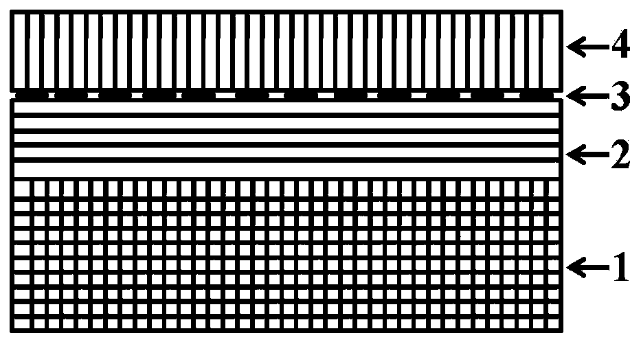
[0069] Such as figure 1 As shown, p-type Cu with a thickness of 300 nm was deposited on the Pt surface of the silicon wafer substrate 1 2 O thin film layer 2, silicon wafer substrate 1 is Pt / Ti / SiO 2 / Si(100); followed by Cu 2A thin gold film layer is deposited on the upper surface of the O film layer 2, and the gold nanorod particle layer 3 is obtained after annealing in the muffle furnace. , gold nanorod particles with a diameter of 10-15nm; finally, in the Cu with gold nanorod particle layer 3 2 A layer of n-type BiFeO with a thickness of 300 nm was deposited on the surface of the O thin film layer 2 3 Ferroelectric thin film layer 4, formed by Cu 2 O / Au / BiFeO 3 photocathode.
PUM
| Property | Measurement | Unit |
|---|---|---|
| thickness | aaaaa | aaaaa |
| length | aaaaa | aaaaa |
| diameter | aaaaa | aaaaa |
Abstract
Description
Claims
Application Information
 - R&D
- Intellectual Property
- Life Sciences
- Materials
- Tech Scout
- Unparalleled Data Quality
- Higher Quality Content
- 60% Fewer Hallucinations
Browse by: Latest US Patents, China's latest patents, Technical Efficacy Thesaurus, Application Domain, Technology Topic, Popular Technical Reports.
© 2025 PatSnap. All rights reserved.Legal|Privacy policy|Modern Slavery Act Transparency Statement|Sitemap|About US| Contact US: help@patsnap.com


