Ferroelectric composite Cu2O visible light water photolysis hydrogen production photocathode and preparing method thereof
A technology for photo-splitting water for hydrogen production and visible light, applied in the field of photoelectrochemistry, can solve the problems of poor photocathode stability, low photo-generated carrier separation and transport efficiency, etc. Effect
- Summary
- Abstract
- Description
- Claims
- Application Information
AI Technical Summary
Problems solved by technology
Method used
Image
Examples
preparation example Construction
[0051] Ferroelectric Composite Cu 2 A preparation method of a photocathode for producing hydrogen by visible light photolysis of water, comprising the following steps:
[0052] Step 1. Place the silicon wafer substrate 1 on the deposition table in the vacuum chamber of the magnetron sputtering apparatus, with the Pt side of the silicon wafer substrate 1 facing up, and the air pressure in the vacuum chamber is 1×10 -4 -3×10 -4 Pa;
[0053] Step 2. Introduce a mixed gas of oxygen and argon with a volume ratio of 1:5-1:6 into the vacuum chamber of step 1, and control the air pressure in the vacuum chamber at 0.75-1Pa;
[0054] Step 3. Adjust the heating power of the magnetron sputtering apparatus to keep the temperature of the deposition table at 250-300° C.;
[0055] Step 4, adjust the sputtering power of the magnetron sputtering apparatus to 30-40W, and deposit Cu on the Pt surface of the silicon wafer substrate 1 2 O thin film layer 2, the deposition time is 20-30min;
[...
Embodiment 1
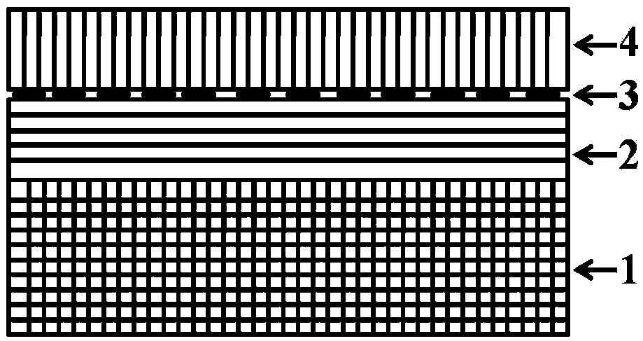
[0069] Such as figure 1 As shown, p-type Cu with a thickness of 300 nm was deposited on the Pt surface of the silicon wafer substrate 1 2 O thin film layer 2, silicon wafer substrate 1 is Pt / Ti / SiO 2 / Si(100); followed by Cu 2A thin gold film layer is deposited on the upper surface of the O film layer 2, and the gold nanorod particle layer 3 is obtained after annealing in the muffle furnace. , gold nanorod particles with a diameter of 10-15nm; finally, in the Cu with gold nanorod particle layer 3 2 A layer of n-type BiFeO with a thickness of 300 nm was deposited on the surface of the O thin film layer 2 3 Ferroelectric thin film layer 4, formed by Cu 2 O / Au / BiFeO 3 photocathode.
PUM
| Property | Measurement | Unit |
|---|---|---|
| Diameter | aaaaa | aaaaa |
| Thickness | aaaaa | aaaaa |
| Photocurrent density | aaaaa | aaaaa |
Abstract
Description
Claims
Application Information
 - R&D
- Intellectual Property
- Life Sciences
- Materials
- Tech Scout
- Unparalleled Data Quality
- Higher Quality Content
- 60% Fewer Hallucinations
Browse by: Latest US Patents, China's latest patents, Technical Efficacy Thesaurus, Application Domain, Technology Topic, Popular Technical Reports.
© 2025 PatSnap. All rights reserved.Legal|Privacy policy|Modern Slavery Act Transparency Statement|Sitemap|About US| Contact US: help@patsnap.com


