Manufacturing method for microchannel heat exchange plate with multi-scale surface structure character
A technology of surface structure and manufacturing method, applied in the field of manufacturing microchannel heat exchange plates, can solve the problems of high cost, complex lithography, high requirements, etc., and achieve the effects of low production cost, simple processing technology and low equipment requirements
- Summary
- Abstract
- Description
- Claims
- Application Information
AI Technical Summary
Problems solved by technology
Method used
Image

Examples
preparation example Construction
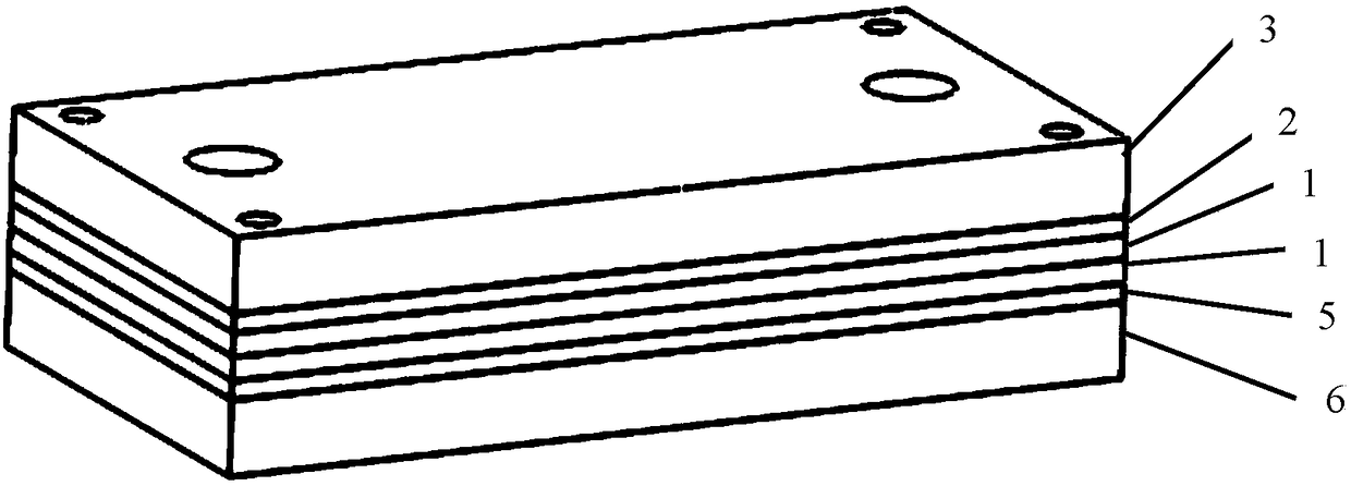
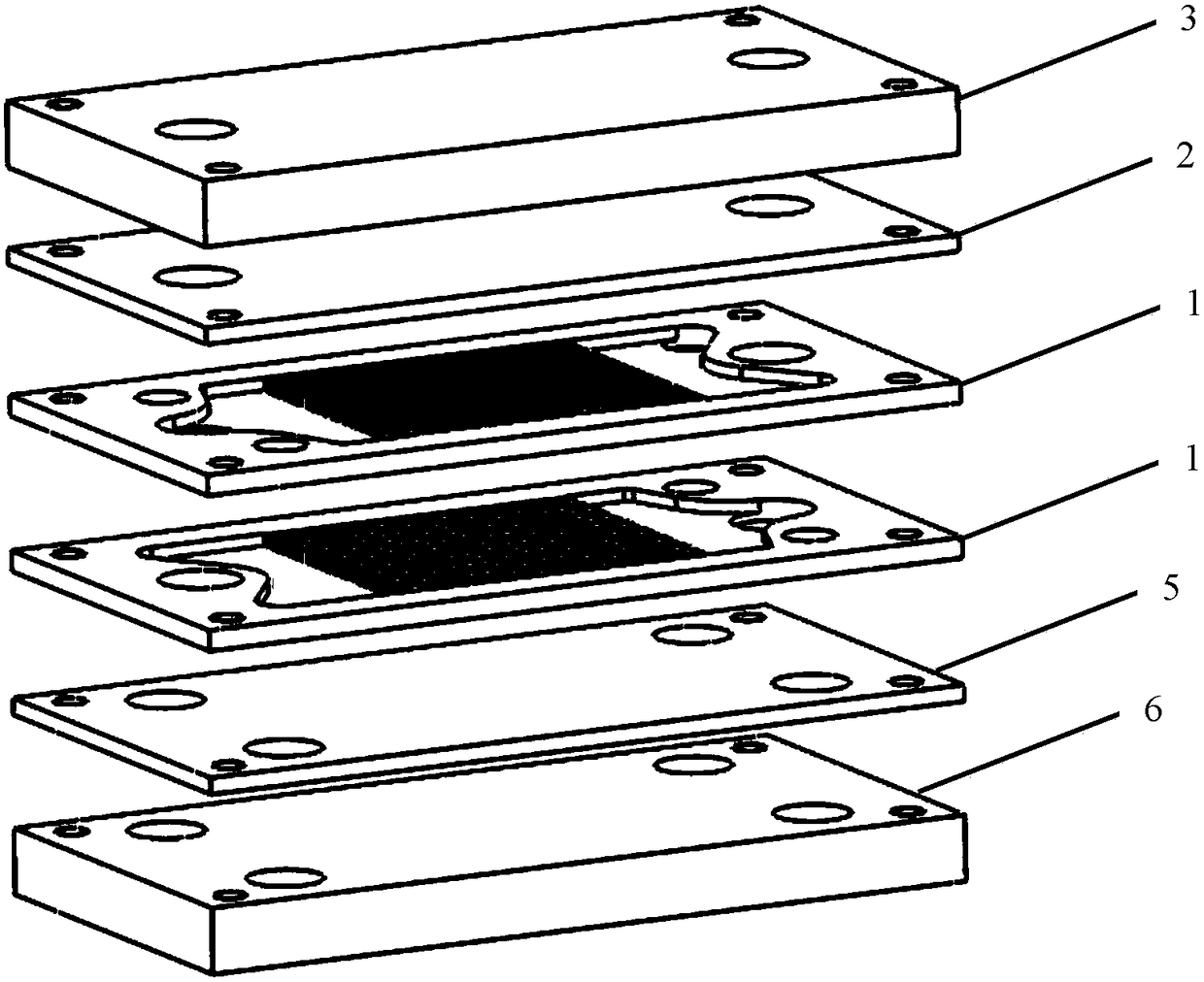
[0028] refer to figure 1 and figure 2 , a microchannel heat exchange plate with multi-scale surface structure features includes an upper cover plate 3, an upper sealing plate 2, two metal substrates 1, a lower sealing plate 5 and a lower cover plate 6, which are stacked sequentially from top to bottom. The substrate 1 is provided with arrayed microchannels 11 with micron-scale features and micro-nano surface structures 12 with smaller bottom scales. Among them, the microchannels 11 are arranged in parallel at equidistant intervals, the interval is 0.4-1.0mm, the width range of each microchannel 11 is 0.2-0.8mm, and the height range is 0.5-2mm; the micro-nano surface structure 12 has regular unevenness, the height 200-500nm. Its preparation method comprises the following steps:
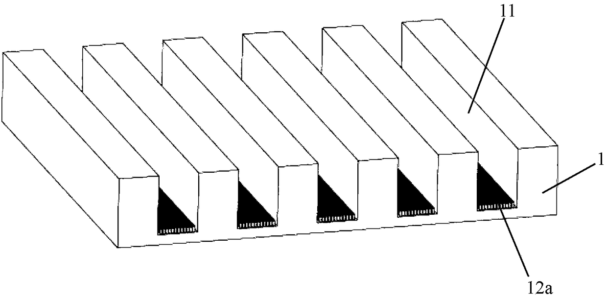
[0029] (1) Use a multi-tooth saw blade milling cutter combination tool to process an arrayed microchannel 11 with micron-scale features on the metal substrate 1 through an ordinary milling machine;...
Embodiment 1
[0033] Provide a red copper plate as the metal substrate 1, and form an array of microchannels 11 on the red copper plate through the above-mentioned multi-tooth saw blade milling cutter combination tool. These microchannels are parallel to each other, with a width range of 0.8mm, a height range of 1mm, and an interval of 0.6mm .
[0034] Using laser processing, the laser wavelength is 1064nm, the average output power of the laser is 30W, the processing speed is 1000mm / s, the number of laser scans for a single microstructure is 30 times, the scanning distance is greater than 0.1mm and the processing path is zigzag scanning , forming a matrix array of nanopillars 12a at the bottom of each microchannel, the interval between adjacent nanopillars is 0.5mm; each nanopillar is a cylinder with a cross-sectional area of 0.2mm 2 . The obtained copper plate structure with multi-scale surface structure features is as follows: image 3 and Figure 4 shown.
[0035] The microchannel ...
Embodiment 2
[0037]Provide a red copper plate, form the arrayed microchannel 11 by the mode of embodiment 1, adopt the mode of laser processing, laser wavelength is 1064nm, the average output power of laser is 30W, processing speed is 1000mm / s, the number of times of laser scan of single microstructure is 30 times, the scanning distance is less than or equal to 0.1mm and the processing path is "back" scanning, forming a matrix-like array of nanopillars 12b at the bottom of each microchannel, the interval between adjacent nanopillars is 0.5mm, and each nanopillar is a cone structure, the bottom area of the cone is 0.2mm 2 . The obtained copper plate structure with multi-scale surface structure features is as follows: Figure 5 shown. The microchannel array structure with multi-scale surface structure features in this embodiment can effectively increase the nucleation points of bubbles, enhance disturbance, and enhance heat transfer.
PUM
| Property | Measurement | Unit |
|---|---|---|
| Height | aaaaa | aaaaa |
| Height | aaaaa | aaaaa |
| Thermal conductivity | aaaaa | aaaaa |
Abstract
Description
Claims
Application Information
 - R&D
- Intellectual Property
- Life Sciences
- Materials
- Tech Scout
- Unparalleled Data Quality
- Higher Quality Content
- 60% Fewer Hallucinations
Browse by: Latest US Patents, China's latest patents, Technical Efficacy Thesaurus, Application Domain, Technology Topic, Popular Technical Reports.
© 2025 PatSnap. All rights reserved.Legal|Privacy policy|Modern Slavery Act Transparency Statement|Sitemap|About US| Contact US: help@patsnap.com