


Quick Research
Generate reliable direction feasibility study reports for your R&D in just a few steps.

Technical Q&A
Discover and master advanced knowledge NOW. Basics, ideas, possibilities, all at once.

Find Solutions
As an expert in R&D theories, this can generate solutions to your technical problems instantly.

Evaluate Feasibility
Analyze your overall solution with one click, know your potential R&D risks in advance.

Monitor Landscape
Get weekly tech updates, stay abreast of the latest tech innovations and key insights.
Method and circuit structure for suppressing single event transients or glitches in digital electronic circuits
A digital electronic circuit, single event transient technology, applied in the direction of improving reliability with backup circuits, logic circuits, failsafe circuits, etc., can solve problems such as long delays
- Summary
- Abstract
- Description
- Claims
- Application Information
AI Technical Summary
Problems solved by technology
Method used
Image


Examples
Embodiment 1
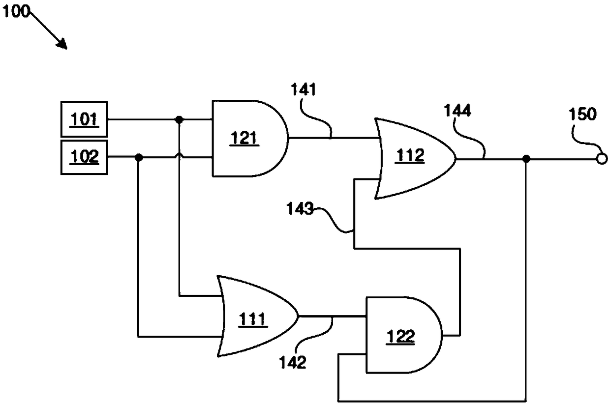
[0070] A circuit (100) as Embodiment 1 is shown in FIG. 1, which has a structure for suppressing SETs or glitches in digital electronic circuits. Terminals of the circuit (100) include a first input (101), a second input (102) and a final circuit output (150). A first input (101) and a second input (102) respectively receive the output of the preceding circuit or sub-circuit and the output of its redundant or repeated circuit.
[0071] The four double-input gates in this embodiment include two OR gates (111, 112) and two AND gates (121, 122).
[0072] Both the first OR gate (111) and the first AND gate (121) receive as inputs the first and second inputs (101, 102) of the circuit. The second OR gate (112) receives the output (141) of the first AND gate (121) as one of its inputs.
[0073] The second AND gate (122) receives the output (142) of the first OR gate (111) as one of its inputs. The second AND gate (122) also receives as its second input the feedback signal of the f...
Embodiment 2
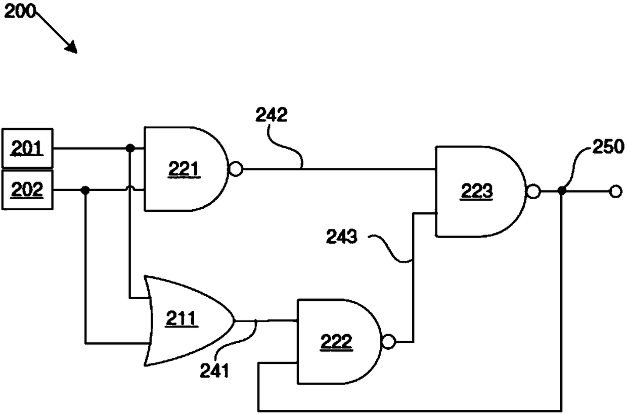
[0081] like figure 2 As shown, in Embodiment 2 of the present invention, the circuit (200) also includes four double-input logic gates, three of which are inverting AND gates (ie NAND gates) (221, 222, 223) and one non-inverting Phase OR gate (211).
[0082] The terminals of the circuit (200) also include a first input (201), a second input (202) and a final output (250). The first input (201) and the second input (202) respectively receive the output of the previous circuit or sub-circuit and the output of its redundant or repeated circuit.
[0083] Both the OR gate (211) and the first NAND gate (221) receive as inputs the first and second inputs (201, 202) of the circuit. The second inverting AND gate (222) receives the output (241) of the non-inverting OR gate (211) as one of its inputs and the feedback signal of the final output (250) of the circuit (200) as its second input.
[0084] The third inverted AND gate (223) receives the output (242) of the first inverted AND...
Embodiment 3
[0091] image 3 Embodiment 3 of the present invention is shown in , and its circuit (300) also includes four double-input logic gates, namely two NAND gates (311, 312), a NOR gate (321) and an OR gate (322 ). Three two-input logic gates are inverting gates while one two-input logic gate is non-inverting gate.
[0092] The terminals of the circuit (300) also include a first input (301), a second input (302) and a final circuit output (350). The first input (301) and the second input (302) respectively receive the output of the previous circuit or sub-circuit and the output of its redundant or repeated circuit.
[0093] Both the NOR gate (321) and the first inverting NAND gate (311) receive as input a feedback signal of the first input (301) and the final output (350) of the circuit (300). The second input (302) is inverted by a single-input NOT gate (303). The inverted signal (341) together with the output (342) of the NOR gate (321) serves as the input of the OR gate (322)...
PUM
 Abstract
Description
Claims
Application Information
 - R&D Engineer
- R&D Manager
- IP Professional
- Industry Leading Data Capabilities
- Powerful AI technology
- Patent DNA Extraction
Browse by: Latest US Patents, China's latest patents, Technical Efficacy Thesaurus, Application Domain, Technology Topic, Popular Technical Reports.
© 2024 PatSnap. All rights reserved.Legal|Privacy policy|Modern Slavery Act Transparency Statement|Sitemap|About US| Contact US: help@patsnap.com