A shielded gate power dmos device

A shielding gate and power technology, applied in the direction of semiconductor devices, electrical components, circuits, etc., can solve the problems of increasing the threshold voltage of power DMOS devices, unable to prevent the parasitic BJT from being turned on, and unable to infinitely reduce the resistance of the parasitic BJT base area, so as to improve the resistance UIS invalidation ability, UIS tolerance improvement, effect of preventing opening

Active Publication Date: 2020-05-26
UNIV OF ELECTRONICS SCI & TECH OF CHINA
View PDF4 Cites 0 Cited by
  • Summary
  • Abstract
  • Description
  • Claims
  • Application Information

AI Technical Summary

Problems solved by technology

However, this method cannot prevent the opening of the parasitic BJT, and it cannot avoid the active failure mode of the device UIS caused by avalanche breakdown; in addition, it can only be reduced to a certain extent by high-energy boron implantation or deep diffusion. The base resistance cannot infinitely reduce the base resistance of the parasitic BJT, otherwise it will increase the threshold voltage of the power DMOS device

Method used


Image

  • A shielded gate power dmos device
  • A shielded gate power dmos device
  • A shielded gate power dmos device

Examples


Embodiment 1

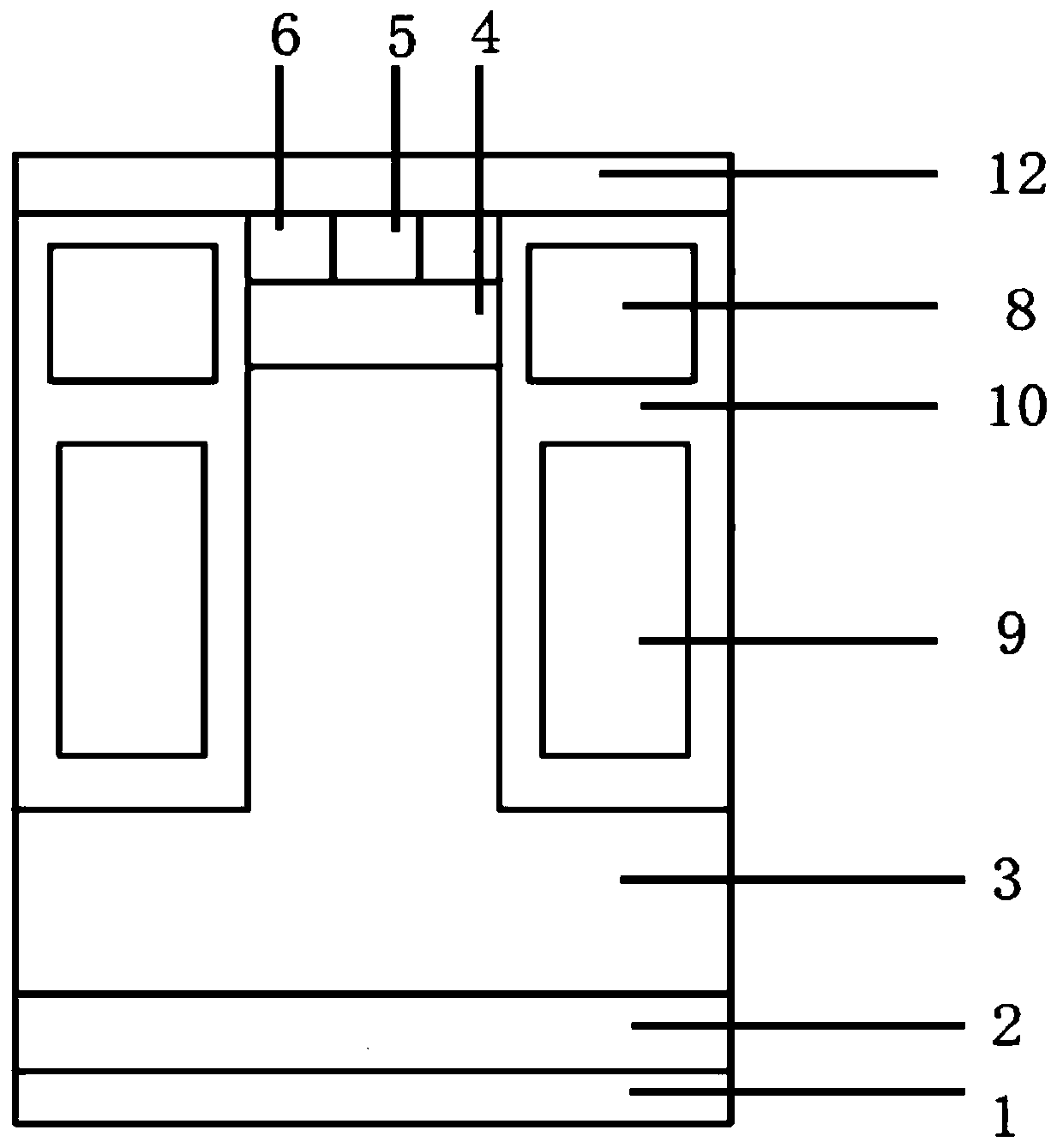
[0026] A shielded gate power DMOS device, the cross-sectional schematic diagram of the cell structure is as figure 2 As shown, it includes: a metalized drain electrode 1, a first conductive type semiconductor substrate 2, a first conductive type semiconductor drift region 3, and a metalized source 12 stacked in sequence from bottom to top, the first conductive type semiconductor A trench gate structure is provided on both sides of the top layer of the drift region 3. The trench gate structure includes a shield gate electrode 9 provided at the bottom of the trench 7, a control gate electrode 8 provided at the top of the trench 7, and a control gate electrode 8 provided at the top of the trench 7. And the dielectric layer 10 around the shielding gate electrode 9, and the control gate electrode 8 and the shielding gate electrode 9 are separated by the dielectric layer 10; the trench gate structure on both sides of the top layer of the first conductivity type semiconductor drift reg...

Embodiment 2

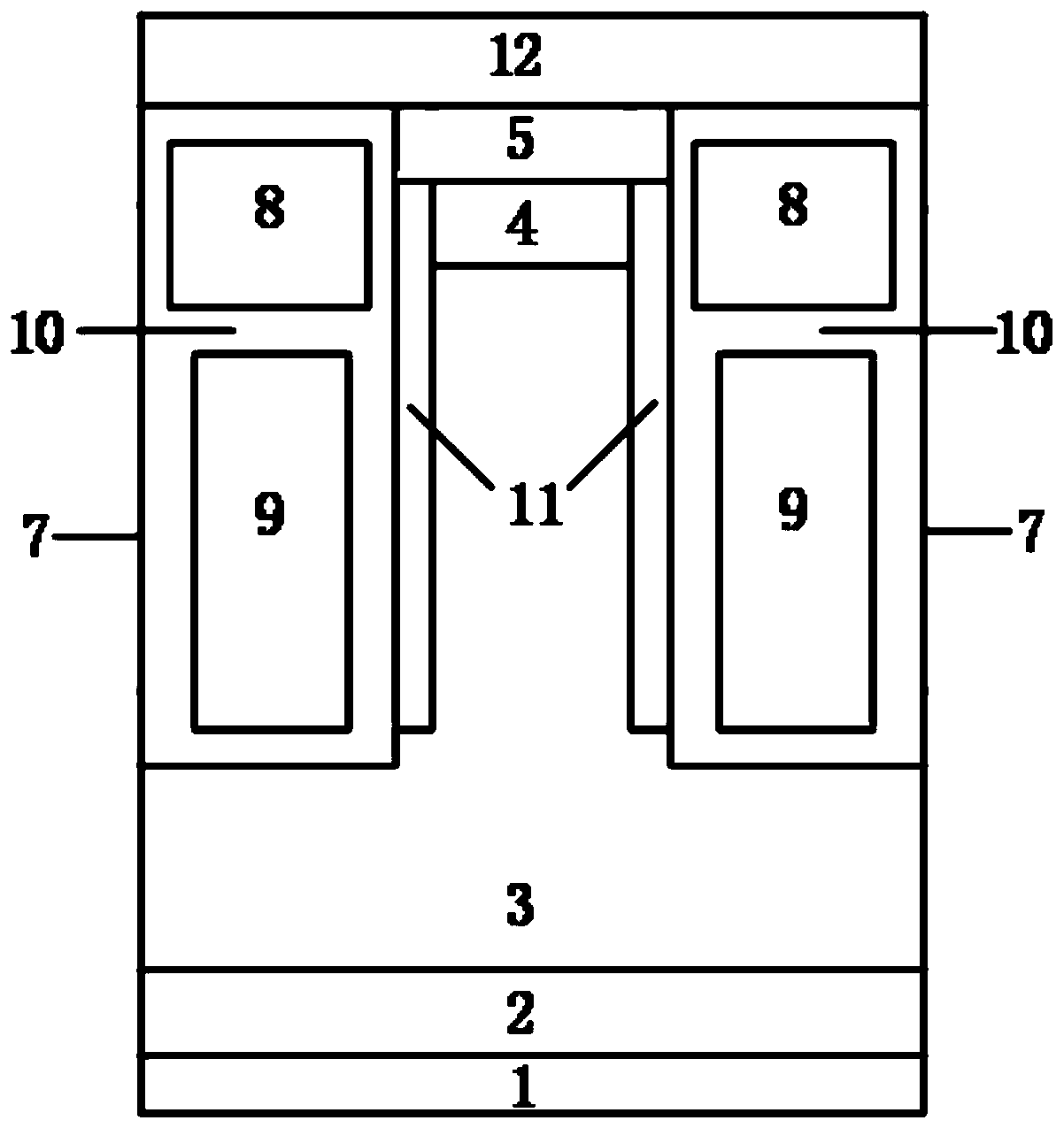
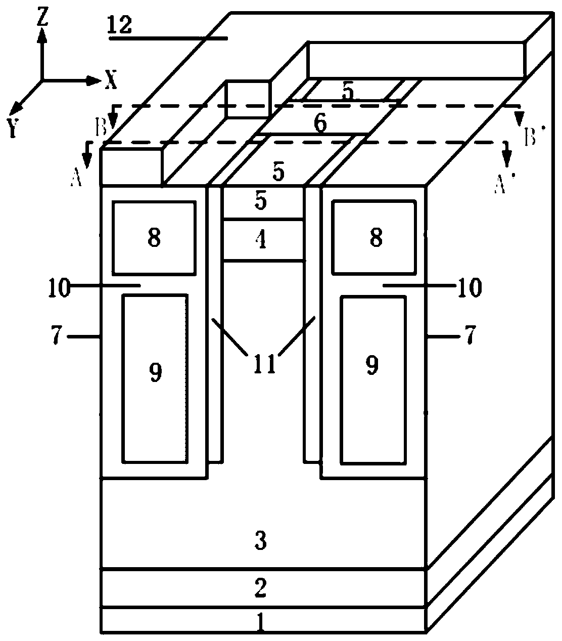
[0028] A shielded gate power DMOS device, the three-dimensional schematic diagram of its cell structure is as image 3 As shown, Figure 4 with Figure 5 The cross-sectional schematic diagrams respectively taken along the AA' line and the BB' line of the cell structure include: including: metallized drain 1, first conductivity type semiconductor substrate 2, first conductivity type stacked in sequence from bottom to top The semiconductor drift region 3 and the metallized source electrode 12. The first conductivity type semiconductor drift region 3 has a trench gate structure on both sides of the top layer, and the trench gate structure includes a shielding gate electrode 9 and a device located at the bottom of the trench 7 The control gate electrode 8 on the top of the trench 7 and the dielectric layer 10 arranged around the control gate electrode 8 and the shielding gate electrode 9 are both along the image 3 The illustrated x-axis direction extends and the two are separated b...


PUM


Abstract

A shielded gate power DMOS device belongs to the technical field of semiconductor power devices. The invention is improved based on the traditional shielded gate DMOS device. The top layer of the drift region between the trench gate structures on both sides of the device has a body region, and the top layer of the body region has alternately arranged source regions and contact regions. Alternate arrangement of the contact regions and the introduction of a heavily doped current guide layer between the contact region and the sidewall of the trench to form a current channel with lower on-resistance, and direct contact between the source region and the dielectric layer on the sidewall of the trench . This design can fix the avalanche breakdown current in the current guide layer, and guide the avalanche current to flow away from the contact area directly through the current guide layer without passing through the body area below the source area, which prevents the parasitic BJT from turning on and improves the The UIS tolerance of the device and the ability to resist UIS failure. In addition, due to the lateral depletion effect of the shielded gate electrode, the negative influence of the current guiding layer on the withstand voltage performance of the device can be avoided.

Description

Technical field [0001] The invention belongs to the technical field of power semiconductor devices, and specifically relates to a shielded gate power DMOS device. Background technique [0002] Power DMOS plays an important role in the field of power conversion due to its advantages such as fast switching speed, low loss, high input impedance, low drive power, and good frequency characteristics. Continuously improving system performance requires power DMOS to have lower power loss and higher reliability under high electrical stress. In order to improve the performance of DMOS, new structures such as floating island unipolar devices and split-gate are proposed. Floating island unipolar devices pass in N - The P-type voltage divider island is added to the epitaxial layer, so that the maximum electric field of the drift region is divided into two parts. Under the same doping concentration of the epitaxial layer, the breakdown voltage is increased; the shielded gate power DMOS uses i...

Claims


Application Information

Patent Timeline
Patent Type & Authority Patents(China)
IPC IPC(8): H01L29/78H01L29/423
CPCH01L29/4236H01L29/7813
Inventor 任敏杨梦琦李佳驹李泽宏高巍张金平张波
Owner UNIV OF ELECTRONICS SCI & TECH OF CHINA
Why Eureka
Try Eureka