Band-gap reference voltage source circuit

A reference voltage source and circuit technology, applied in the direction of adjusting electrical variables, control/regulating systems, instruments, etc., can solve the problems of variation, chip deviation, VBG inaccuracy, etc., and achieve the effect of high output voltage accuracy

Active Publication Date: 2018-07-24
NANJING ZGMICRO CO LTD
View PDF8 Cites 2 Cited by
  • Summary
  • Abstract
  • Description
  • Claims
  • Application Information

AI Technical Summary

Problems solved by technology

[0003] Although Q1 is designed as K transistors in parallel with Q2, there is a mismatch between each transistor in Q1 and Q2, that is, when mass production, there will be differences between chips, and these differences will cause inaccurate VBG, And this difference will vary due to package stress effects
Even at the wafer or chip stage, VBG is adjusted accurately through trimming technology, but after packaging, due to the influence of packaging stress, there are deviations between chips

Method used


Image

  • Band-gap reference voltage source circuit
  • Band-gap reference voltage source circuit
  • Band-gap reference voltage source circuit

Examples


Embodiment Construction

[0020] In order to make the above objects, features and advantages of the present invention more comprehensible, the present invention will be further described in detail below in conjunction with the accompanying drawings and specific embodiments.

[0021] Reference herein to "one embodiment" or "an embodiment" refers to a particular feature, structure or characteristic that can be included in at least one implementation of the present invention. "In one embodiment" appearing in different places in this specification does not all refer to the same embodiment, nor is it a separate or selective embodiment that is mutually exclusive with other embodiments. Unless otherwise specified, the words connected, connected, and joined in this document mean that they are electrically connected directly or indirectly.

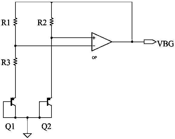
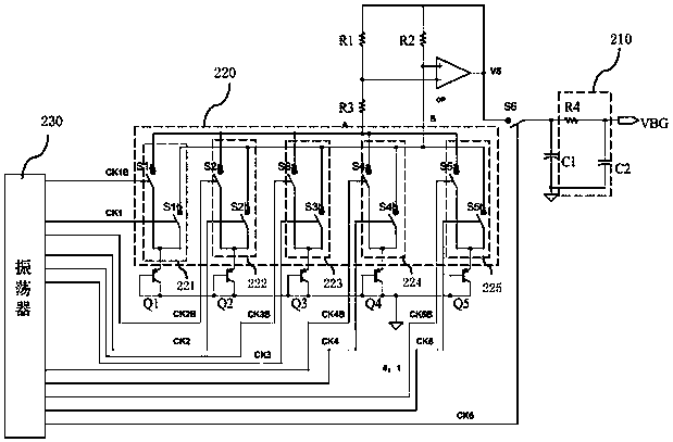
[0022] Please refer to figure 2 As shown, it is a schematic circuit diagram of a bandgap reference voltage source circuit in an embodiment of the present invention. fig...


PUM


Abstract

The invention provides a band-gap reference voltage source circuit. The band-gap reference voltage source circuit comprises an operation amplifier, a third resistor, a first node, a second node, a sampling switch, a first capacitor, a filter, a switch combination circuit, N bipolar transistors, a second resistor, a first MOS transistor and a second MOS transistor. The first input end of the operation amplifier is connected with the second middle node, the second input end of the operation amplifier is connected with the first node through the third resistor, and the output end of the operationamplifier is grounded after passing through the sampling switch and the first capacitor in sequence. The first connecting ends of all the bipolar transistors are connected with the switch combinationcircuit, the second connecting ends of all the bipolar transistors are connected with the control ends of the bipolar transistors themselves and are grounded, and the switch combination circuit makesthe first connecting ends of all the bipolar transistors selectively connected with the first node or the second node. Compared with the prior art, the band-gap reference voltage source circuit can further improve the precision of output reference voltage.

Description

【Technical field】 [0001] The invention relates to the technical field of electronic circuits, in particular to a bandgap reference voltage source circuit. 【Background technique】 [0002] Bandgap reference voltage sources are widely used in various analog circuits. In practical applications, high-precision bandgap reference voltage sources are favored. Please refer to figure 1 As shown, it is a schematic circuit diagram of a bandgap reference voltage source in the prior art, which includes resistors R1, R2, R3, bipolar transistors PNP transistors Q1, Q2, and an operational amplifier OP. Generally, the emitter area of ​​Q1 is designed to be larger than that of Q2, for example, its ratio is K:1. In order to achieve a better matching effect in actual design, Q1 is generally designed as K PNP transistors in parallel with Q2. In one example K=4. Generally, the resistance values ​​of resistors R1 and R2 are designed to be the same, and are designed to be M times the resistance ...

Claims


Application Information

Patent Timeline
Patent Type & Authority Applications(China)
IPC IPC(8): G05F1/56
CPCG05F1/56
Inventor 王钊
Owner NANJING ZGMICRO CO LTD
Why Eureka
Try Eureka