Double-node upset prevention latch
A technology of double-node flipping and latches, which is applied to the coupling/interface of logic circuits using field effect transistors, reliability improvement modification, logic circuits, etc., and can solve the problem that latches cannot resist double-node flipping, low area overhead, etc. problem, to achieve the effect of improving the ability to resist single event flipping, low area overhead, and high reliability
- Summary
- Abstract
- Description
- Claims
- Application Information
AI Technical Summary
Problems solved by technology
Method used
Image


Examples
Embodiment 1
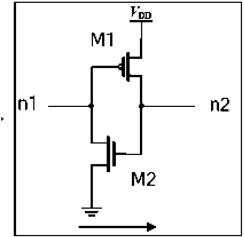
[0022] figure 1 It is a schematic structural diagram of a latch resistant to double-node flipping provided by an embodiment of the present application. like figure 1 shown, the latch consists of:
[0023] The latch has a storage node A, a storage node B, a storage node C, a storage node D, a storage node E, and a storage node F;
[0024] Specifically, a latch (Latch) is a memory unit circuit sensitive to a pulse level, and they can change states under the action of a specific input pulse level. Latch is to temporarily store the signal to maintain a certain level state. The main function of the latch is to cache, secondly to complete the asynchronous problem between the high-speed controller and the slow peripheral, then to solve the problem of the driver, and finally to solve the problem that an I / O port can output and input question. A latch is an input that uses level control data, and it includes a latch without enable control and a latch with enable control. The stor...
Embodiment 2
[0029] The embodiment of the present application also provides a latch that resists double-node flipping, and the latch includes:
[0030] The latch has a storage node A, a storage node B, a storage node C, a storage node D, a storage node E, and a storage node F;
[0031] The latch also has: a first cross-coupling structure 1, the input terminal of the first cross-coupling structure 1 is connected to the storage node A, and the output terminal is connected to the storage node B; a second cross-coupling structure 2, the second cross-coupling structure 2 The input terminal of the coupling structure 2 is connected to the storage node C, and the output terminal is connected to the storage node A; the third cross-coupling structure 3, the input terminal of the third cross-coupling structure 3 is connected to the storage node F, and the output terminal is connected to the storage node C; the fourth The cross-coupling structure 4, the input terminal of the fourth cross-coupling stru...
Embodiment 3
[0034] In order to further explain the anti-double-node flipping latch provided in the present application, the embodiment of the present application describes the working principle of the anti-double-node flipping latch.
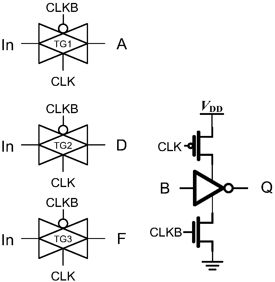
[0035] When the latch is in conduction mode, as image 3 As shown, the input data In is transmitted to the storage node A, the storage node D and the storage node F respectively through the CMOS transmission gates TG1, TG2 and TG3, while the storage node B, the storage node E and the storage node C are logically opposite to the input data In. The storage node B outputs to the output node Q through a clocked inverter, so the input In is logically the same as the output Q. When the latch is in the holding mode, these redundant storage nodes have the ability to restore correct logic, which improves the ability of digital integrated circuits to resist single event flipping under harsh conditions, resist double-node flipping, and have high reliability and low co...
PUM
 Abstract
Description
Claims
Application Information
 - R&D
- Intellectual Property
- Life Sciences
- Materials
- Tech Scout
- Unparalleled Data Quality
- Higher Quality Content
- 60% Fewer Hallucinations
Browse by: Latest US Patents, China's latest patents, Technical Efficacy Thesaurus, Application Domain, Technology Topic, Popular Technical Reports.
© 2025 PatSnap. All rights reserved.Legal|Privacy policy|Modern Slavery Act Transparency Statement|Sitemap|About US| Contact US: help@patsnap.com