
MRAM (Magnetic Random Access Memory) reading circuit using low-voltage pulse

A technology of reading out circuits and low-voltage pulses, used in information storage, static memory, digital memory information, etc.

Active Publication Date: 2018-06-08
SHANGHAI CIYU INFORMATION TECH
View PDF6 Cites 1 Cited by
  • Summary
  • Abstract
  • Description
  • Claims
  • Application Information

AI Technical Summary

Problems solved by technology

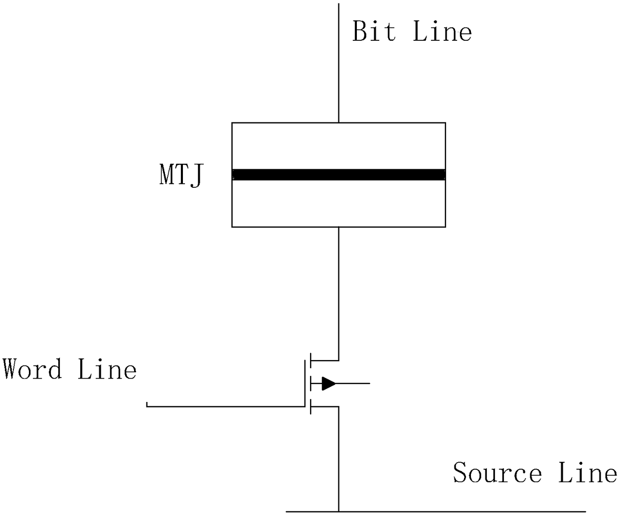
When measuring the resistance of a memory cell, direct current is unavoidable, and the power consumption of this readout circuit accounts for most of the MRAM read power consumption.

Method used


Image

  • MRAM (Magnetic Random Access Memory) reading circuit using low-voltage pulse
  • MRAM (Magnetic Random Access Memory) reading circuit using low-voltage pulse
  • MRAM (Magnetic Random Access Memory) reading circuit using low-voltage pulse

Examples


Embodiment Construction

[0032] The preferred embodiments of the present invention are described in detail below, so that the advantages and features of the present invention can be more easily understood by those skilled in the art, so as to define the protection scope of the present invention more clearly.

[0033] Such as Figure 5 As shown, an MRAM readout circuit using low-voltage pulses includes a plurality of equivalent MOS transistors arranged in a row, a reference unit combination and a comparator.

[0034] A plurality of equivalent MOS transistors arranged in a row are connected in parallel and divided into two groups, the first group is Pb1, Pb2...Pbk, and the second group is Pax (x=1, 2,...).

[0035] The reference cell combination consists of k reference cells connected in parallel, some of the k reference cells are configured in the P state, and the rest are configured in the AP state, and the reference cells are divided into multiple columns and placed in the MRAM memory cell array.

...


PUM


Abstract

The invention discloses an MRAM (Magnetic Random Access Memory) reading circuit using a low-voltage pulse. The reading circuit comprises a plurality of equivalent MOS (Metal Oxide Semiconductor) transistors, a reference unit combination and a comparator which are arranged in a row and connected in parallel; in the plurality of MOS transistors, k MOS transistors are connected in parallel and then connected with k reference units of the reference unit combination in series; each remaining MOS transistor Pax in the plurality of MOS transistors is connected with a read storage unit in series; thecomparator is located between the Ax and B points; and whether the storage unit is in a P state or an AP state is determined through a voltage difference between the two points. According to the MRAMreading circuit using the low-voltage pulse, a read operation is performed by use of the low-voltage pulse, and the read power consumption of the MRAM reading circuit is effectively reduced.

Description

technical field [0001] The invention belongs to the field of semiconductor chip memory, in particular to an MRAM readout circuit using low-voltage pulses. Background technique [0002] Magnetic Random Access Memory (MRAM) is an emerging non-volatile storage technology. It has high-speed read and write speed and high integration, and can be rewritten infinitely. MRAM can be read and written as fast as SRAM / DRAM, and can permanently retain data after power failure like Flash memory. [0003] MRAM has very good economy and performance. Its silicon chip area occupied per unit capacity has great advantages over SRAM, and also has advantages over NOR Flash, which is often used in such chips, and has greater advantages than embedded NOR Flash. . The MRAM read and write delay is close to the best SRAM, and the power consumption is the best among various memory and storage technologies; and MRAM is compatible with standard CMOS semiconductor processes, while DRAM and Flash are not...

Claims


Application Information

Patent Timeline
IPC IPC(8): G11C11/16
CPCG11C11/161G11C11/1673
Inventor 戴瑾
Owner SHANGHAI CIYU INFORMATION TECH
Learn More