


Quick Research
Generate reliable direction feasibility study reports for your R&D in just a few steps.

Technical Q&A
Discover and master advanced knowledge NOW. Basics, ideas, possibilities, all at once.

Find Solutions
As an expert in R&D theories, this can generate solutions to your technical problems instantly.

Evaluate Feasibility
Analyze your overall solution with one click, know your potential R&D risks in advance.

Monitor Landscape
Get weekly tech updates, stay abreast of the latest tech innovations and key insights.
LED packaging method
A technology for LED packaging and LED chips, applied in semiconductor devices, electrical components, circuits, etc., can solve the problems of decreased quantum efficiency of phosphor powder, decreased light intensity, decreased LED service life, etc. cost, improve the effect of luminous dispersion
- Summary
- Abstract
- Description
- Claims
- Application Information
AI Technical Summary
Problems solved by technology
Method used
Image

Examples
Embodiment 1
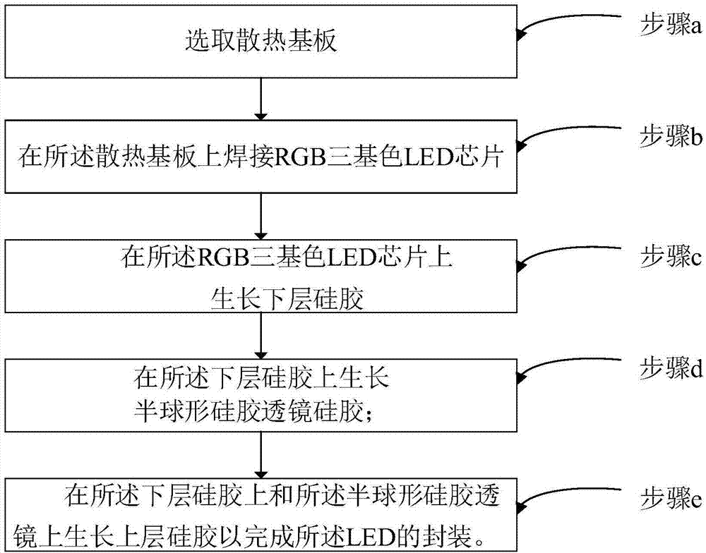
[0050] See figure 1 , figure 1 It is a flow chart of an LED packaging method provided by an embodiment of the present invention. The method comprises the steps of:
[0051] Step a, selecting a heat dissipation substrate;
[0052] Step b, soldering RGB tricolor LED chips on the heat dissipation substrate;
[0053] Step c, growing a lower layer of silica gel on the RGB tricolor LED chip;
[0054] Step d, growing a hemispherical silica gel lens on the lower layer of silica gel;
[0055] Step e, growing an upper layer of silica gel on the lower layer of silica gel and the hemispherical silica gel lens to complete the packaging of the LED.
[0056] Preferably, the heat dissipation substrate is made of aluminum with a thickness of 0.5-10 mm.
[0057] Preferably, circular through holes are provided in the heat dissipation substrate, and the circular through holes are arranged in the width direction inside the heat dissipation substrate and form an angle of 1-10° with the plane of...
Embodiment 2
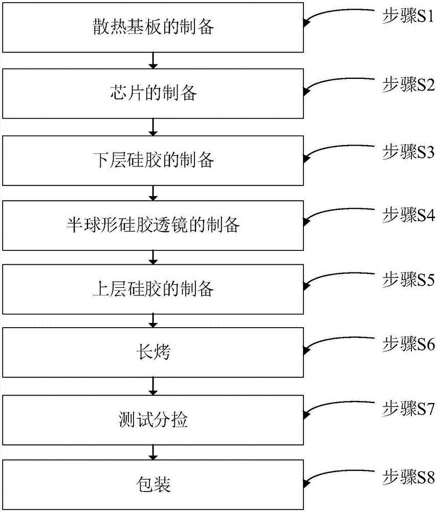
[0085] See figure 2 , figure 2 It is a schematic flow chart of an LED packaging method provided by an embodiment of the present invention. On the basis of the above embodiments, this embodiment will introduce the process flow of the present invention in more detail. The method includes:
[0086] S1, preparation of heat dissipation substrate;
[0087] S11, preparation of support / radiation substrate;
[0088] Specifically, select a heat dissipation substrate 101 whose thickness is 0.5-10 mm and whose material is aluminum, and cut the heat dissipation substrate 101;
[0089] S12. Cleaning of the support / heat dissipation substrate;
[0090] Specifically, clean the stains on the heat dissipation substrate 101 and the support, especially the oil stains;
[0091] S13, baking of the bracket / radiation substrate;
[0092] Specifically, the cleaned heat dissipation substrate 101 and the support are baked to keep the heat dissipation substrate 101 and the support dry.
[0093] P...
Embodiment 3
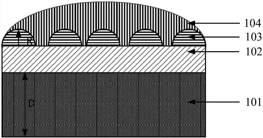
[0121] Please also see image 3 , Figure 4 , Figure 5 and Figure 6a ~ Figure 6b , image 3 A schematic cross-sectional view of an LED package structure provided by an embodiment of the present invention, Figure 4 It is a schematic diagram of the structural principle of an RGB three-color LED chip provided by an embodiment of the present invention, Figure 5 A schematic cross-sectional view of a heat dissipation substrate provided by an embodiment of the present invention, Figure 6a A schematic cross-sectional view of a spherical silicone lens provided by an embodiment of the present invention, Figure 6b A schematic cross-sectional view of another spherical silicone lens provided by an embodiment of the present invention. On the basis of the above embodiments, this embodiment will introduce the LED packaging structure of the present invention, and the LED packaging structure includes:
[0122] heat dissipation substrate 101;
[0123] Among them, such as Figure 5 A...
PUM
 Abstract
Description
Claims
Application Information
 - R&D Engineer
- R&D Manager
- IP Professional
- Industry Leading Data Capabilities
- Powerful AI technology
- Patent DNA Extraction
Browse by: Latest US Patents, China's latest patents, Technical Efficacy Thesaurus, Application Domain, Technology Topic, Popular Technical Reports.
© 2024 PatSnap. All rights reserved.Legal|Privacy policy|Modern Slavery Act Transparency Statement|Sitemap|About US| Contact US: help@patsnap.com