MRAM chip

A chip and array technology, applied in the field of MRAM chips, can solve the problems of insufficient source line width, low power efficiency, and inability to provide, and achieve the effect of solving insufficient power supply, reducing energy consumption, and reducing the probability of continuous errors

Inactive Publication Date: 2018-04-24
SHANGHAI CIYU INFORMATION TECH
View PDF3 Cites 1 Cited by
  • Summary
  • Abstract
  • Description
  • Claims
  • Application Information

AI Technical Summary

Problems solved by technology

[0024] ·Because a fixed voltage drop is required on the memory cell when writing, the voltage difference between the high potential and the low potential required by this method is twice that of the parallel layout scheme between the bit line and the source line, and the chip requires the use of an external Unable to provide high voltage or negative voltage, both of which require internally designed circuits to generate different voltages, and voltage conversion will result in reduced power efficiency and additional costs;
[0025] When writing, the current required for the entire row flows in from the same bit line, and it is often difficult to design because the width of the source line is not enough

Method used


Image

  • MRAM chip
  • MRAM chip
  • MRAM chip

Examples


Embodiment Construction

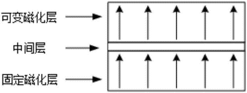
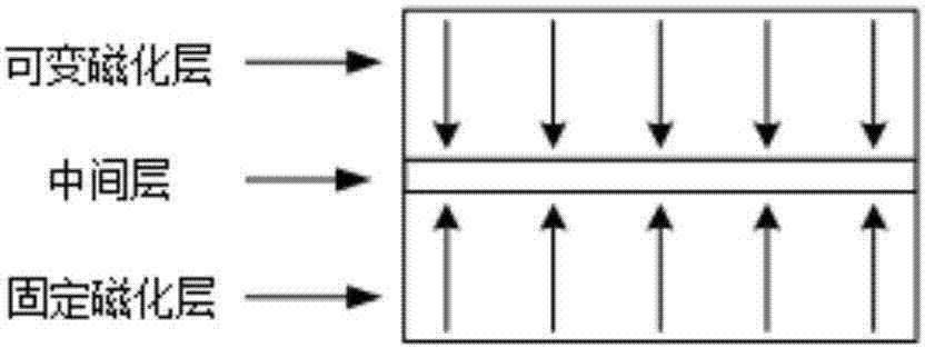
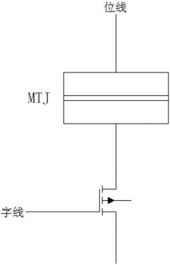
[0046] The MRAM chip of an embodiment of the present invention includes a plurality of arrays composed of MRAM memory cells, each array adopts a vertical layout of bit lines and source lines, and each bit in each word is stored in a different array respectively , each array stores one bit.

[0047] Because an array only writes one bit at a time, high voltage or negative voltage is no longer needed, so that the array design is simple and the energy consumption is reduced, and the problem of insufficient power supply of the source line is solved.

[0048] Each array includes a sense amplifier. Since an array only writes one bit at a time, all bit lines in the same row in the array share the sense amplifier, further reducing the cost of the MRAM chip.

[0049] Two adjacent rows in the array share a source line, such as Figure 7 As shown, the area occupied by the layout is further reduced, and the cost of the MRAM chip is reduced.

[0050] Each word can also include ECC error c...


PUM


Abstract

The invention provides an MRAM chip. The MRAM chip comprises a plurality of arrays formed by MRAM storage units, wherein each array adopts a layout in which bit lines are vertical to source lines; bits in each character are respectively stored in different arrays; each array stores one bit. According to the MRAM chip, the bit lines are vertical to the source lines; the bits in each character are respectively stored in a plurality of arrays; each array only writes one bit at each time, so that high voltage or negative voltage is not needed, the arrays are simple to design, the energy consumption is reduced, and the problem that the source lines are insufficient in power supply is solved; all the bits in a same line in the arrays share a read amplifier, and one array only needs one read amplifier, so that the cost of MRAM chip is reduced; and when ECC is used in error correction, different bits of a same character do not have adjacent positions, so that the probability of continuous errors is reduced, errors can be correctly corrected by ECC, and the reliability of the MRAM chip is improved.

Description

technical field [0001] The invention belongs to the field of semiconductor chips, and in particular relates to an MRAM chip. Background technique [0002] About MRAMs: [0003] The background of the present invention is the maturity of MRAM technology. MRAM is a new memory and storage technology that can be read and written as fast as SRAM / DRAM, and can permanently retain data after power failure like Flash memory. [0004] Its economy is ideally good, and the silicon chip area occupied per unit capacity has a great advantage over SRAM, and also has advantages over NOR Flash, which is often used in such chips, and has greater advantages than embedded NOR Flash. Its performance is also quite good, the read and write latency is close to the best SRAM, and the power consumption is the best among various memory and storage technologies. Moreover, MRAM is not compatible with standard CMOS semiconductor processes like DRAM and Flash. MRAM can be integrated into a chip with log...

Claims


Application Information

Patent Timeline
IPC IPC(8): G11C11/16
CPCG11C11/1697
Inventor 戴瑾俞华樑叶力郭一民陈峻
Owner SHANGHAI CIYU INFORMATION TECH
Why Eureka
Try Eureka