Novel broadband PCB antenna suitable for Wireless Local Area Network (WLAN)

A PCB antenna and wireless local area network technology, which is applied in the field of WLAN dual-band antennas using broadband technology, can solve problems such as narrow frequency band bandwidth, achieve good robustness, strong robustness, and expand the overall bandwidth.

Pending Publication Date: 2018-04-20
SHANGHAI RADIATE COMM ELECTRONICS
View PDF0 Cites 4 Cited by
  • Summary
  • Abstract
  • Description
  • Claims
  • Application Information

AI Technical Summary

Problems solved by technology

However, the traditional PCB antenna design scheme needs to place the antenna position in the clearance area on the edge of the motherboard, and the frequency band bandwidth is narrow, which is greatly affected by the complex use environment

Method used


Image

  • Novel broadband PCB antenna suitable for Wireless Local Area Network (WLAN)
  • Novel broadband PCB antenna suitable for Wireless Local Area Network (WLAN)
  • Novel broadband PCB antenna suitable for Wireless Local Area Network (WLAN)

Examples


Embodiment Construction

[0018] In order to illustrate the technical solutions of the embodiments of the present invention more clearly and effectively, the technical solutions will be described in conjunction with the drawings and embodiments.

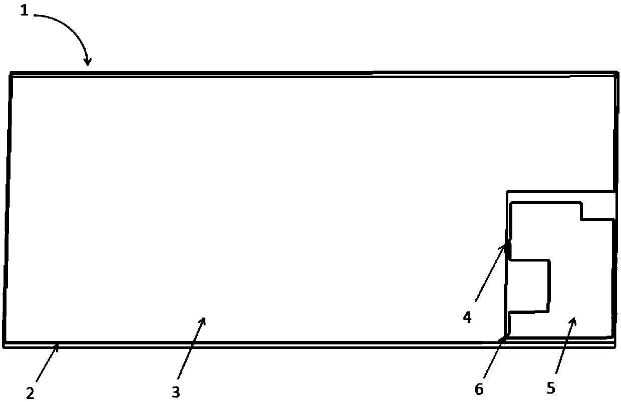
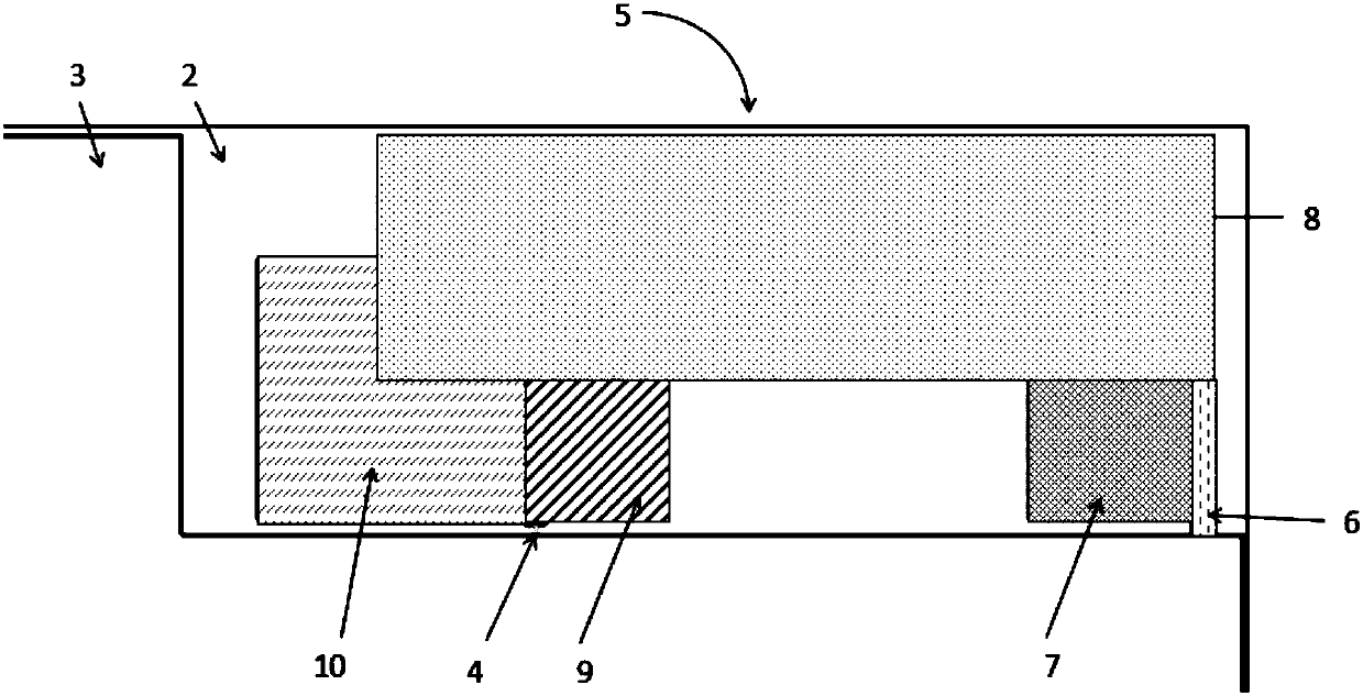
[0019] Such as figure 1 with figure 2 As shown, the PCB antenna of this broadband WLAN is located at the corner of the printed circuit board. The new WLAN antenna includes: a dielectric substrate 2 , a metal ground plate 3 , a feeding point 4 , and an antenna radiation unit 5 . Wherein, the antenna radiation unit includes a ground wire 6, a first radiator 7, a second radiator 8, a third radiator 9, and a fourth radiator 10; the antenna radiation unit is located on a printed circuit board, and the printed circuit board as a whole As an antenna system, see Figure 1 with Figure II .

[0020] The antenna radiating unit 5 is located at a corner of the printed circuit board 1, and its two sides are surrounded by the metal ground plate 3 of the printed circu...


PUM


Abstract

The invention relates to a novel broadband PCB antenna suitable for a Wireless Local Area Network (WLAN). The novel broadband PCB antenna includes a printed circuit board and an antenna radiation unit, the antenna radiation unit is located on the printed circuit board, the antenna radiation unit and the printed circuit board serve as antenna system, a grounding wire is located on an edge of the antenna radiation unit and the printed circuit board, a first radiating body is arranged beside the grounding wire, and a second radiating body, the grounding wire and a third radiating body form a broadband loop antenna; the third radiating body is coupled to a lower side metal floor plate; a fourth radiating body serves as a branch line of an antenna radiating body and is located at an included angle position of two side faces of the metal floor plate. Three principles of forming the loop antenna, antenna branch line and antenna ground coupling are utilized to realize broadband radiation impedance, thereby realizing antenna effective radiation in an ultra-wide range of 1.36GHz to 8GHz, covering a WLAN 2.4GHz frequency band and a 5GHz frequency band, and having very high robustness to surrounding environment of the antenna.

Description

technical field [0001] The invention belongs to a WLAN broadband PCB antenna suitable for a wireless local area network, in particular to a WLAN dual-band antenna realized by using broadband technology. Background technique [0002] Wireless Local Area Network, WLAN uses radio frequency technology to replace old cables with electromagnetic waves to form a wireless data transmission network, which is widely used in smartphones, tablet computers and other communication devices. Wireless local area network users can connect to the wireless access node Access Point, AP through the handheld device, thereby accessing the wireless local area network. The AP antenna in the WLAN is an important part of the entire communication system. Common AP built-in WLAN antennas are mostly attached to PCB boards. This traditional built-in AP antenna is greatly affected by the environment. In order to be used for WLAN network coverage in different places, AP devices often need to be distributed...

Claims


Application Information

Patent Timeline
IPC IPC(8): H01Q1/36H01Q1/38H01Q1/48H01Q1/50H01Q5/10H01Q5/28H01Q7/00
CPCH01Q1/36H01Q1/38H01Q1/48H01Q1/50H01Q5/10H01Q5/28H01Q7/00
Inventor 王坤栗文坤林规
Owner SHANGHAI RADIATE COMM ELECTRONICS
Why Eureka
Try Eureka