


Quick Research
Generate reliable direction feasibility study reports for your R&D in just a few steps.

Technical Q&A
Discover and master advanced knowledge NOW. Basics, ideas, possibilities, all at once.

Find Solutions
As an expert in R&D theories, this can generate solutions to your technical problems instantly.

Evaluate Feasibility
Analyze your overall solution with one click, know your potential R&D risks in advance.

Monitor Landscape
Get weekly tech updates, stay abreast of the latest tech innovations and key insights.
LED packaging structure
A packaging structure, silica gel technology, applied in the direction of semiconductor devices, electrical components, circuits, etc., can solve the problems that affect the heat dissipation effect, the bottom surface of the heat sink is not in close contact, and affect the light transmission efficiency, so as to solve the problem of light transmittance decline and improve heat dissipation effect, the effect of reducing manufacturing cost
- Summary
- Abstract
- Description
- Claims
- Application Information
AI Technical Summary
Problems solved by technology
Method used
Image


Examples
Embodiment 1
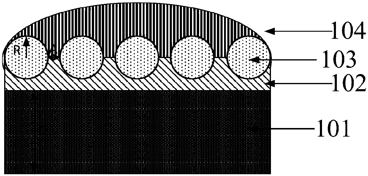
[0041] See figure 1 , figure 1 It is a schematic cross-sectional view of an LED packaging structure provided by an embodiment of the present invention. The structure includes:
[0042] Heat dissipation substrate 101;
[0043] The ultraviolet chip is located on the upper surface of the heat dissipation substrate 101;
[0044] The lower layer of silica gel 102 is located on the upper surface of the ultraviolet chip and the heat dissipation substrate 101;
[0045] The upper layer of silica gel 104 is located on the upper surface of the lower layer of silica gel 102;
[0046] The spherical silica gel lenses 103 are arranged at intervals at the interface between the lower silica gel 102 and the upper silica gel 104.
[0047] Further, the material of the heat dissipation substrate 101 is iron.
[0048] Further, the thickness of the heat dissipation substrate 101 is 0.5-10 mm.
[0049] Further, a circular through hole is provided in the heat dissipation substrate 101; wherein the central line of...
Embodiment 2
[0064] See figure 2 , figure 2 It is a schematic flow diagram of an LED packaging method provided by an embodiment of the present invention. On the basis of the foregoing embodiment, this embodiment will introduce the process flow of the present invention in more detail. The method includes:
[0065] S1. Preparation of heat dissipation substrate;
[0066] S11. Preparation of support / heat dissipation substrate;
[0067] Specifically, a heat dissipation substrate 101 with a thickness of 0.5-10 mm and a material of iron is selected, and the heat dissipation substrate 101 is cut;
[0068] S12. Cleaning of support / heat dissipation substrate;
[0069] Specifically, clean the stains, especially oil stains, on the heat dissipation substrate 101 and the bracket;
[0070] S13. Baking of support / heat dissipation substrate;
[0071] Specifically, the heat-dissipating substrate 101 and the bracket that have been cleaned are baked to keep the heat-dissipating substrate 101 and the bracket dry.
[00...
Embodiment 3
[0111] See also image 3 , Figure 4 , Figure 5 , Image 6 , Figure 7a ~ Figure 7b , image 3 Is a schematic cross-sectional view of an LED package structure provided by an embodiment of the present invention, Figure 4 Is a schematic cross-sectional view of another LED package structure provided by an embodiment of the present invention, Figure 5 Is a schematic cross-sectional view of a heat dissipation substrate provided by an embodiment of the present invention, Image 6 Is a schematic cross-sectional view of an ultraviolet wick provided by an embodiment of the present invention, Figure 7a Is a schematic cross-sectional view of a spherical silicone lens provided by an embodiment of the present invention, Figure 7b It is a schematic cross-sectional view of another spherical silica gel lens provided by an embodiment of the present invention. Heat dissipation substrate 101;
[0112] Among them, such as Figure 5 As shown, the material of the heat dissipation substrate 101 is i...
PUM
 Abstract
Description
Claims
Application Information
 - R&D Engineer
- R&D Manager
- IP Professional
- Industry Leading Data Capabilities
- Powerful AI technology
- Patent DNA Extraction
Browse by: Latest US Patents, China's latest patents, Technical Efficacy Thesaurus, Application Domain, Technology Topic, Popular Technical Reports.
© 2024 PatSnap. All rights reserved.Legal|Privacy policy|Modern Slavery Act Transparency Statement|Sitemap|About US| Contact US: help@patsnap.com