
Package structures

A technology of packaging structure and packaging materials, applied in the direction of semiconductor/solid-state device parts, semiconductor devices, electrical components, etc., can solve the problem of poor heat dissipation effect of copper clips, achieve good heat dissipation, improve component efficiency, and reduce package size Effect

Pending Publication Date: 2018-04-10
DELTA ELECTRONICS INC
View PDF4 Cites 0 Cited by
  • Summary
  • Abstract
  • Description
  • Claims
  • Application Information

AI Technical Summary

Problems solved by technology

[0006] However, the solid copper bridges (such as copper clips) used in clip bonding packages are also encapsulated by packaging materials, resulting in poor heat dissipation of the packaged copper clips.

Method used


Image

  • Package structures
  • Package structures
  • Package structures

Examples


Embodiment Construction

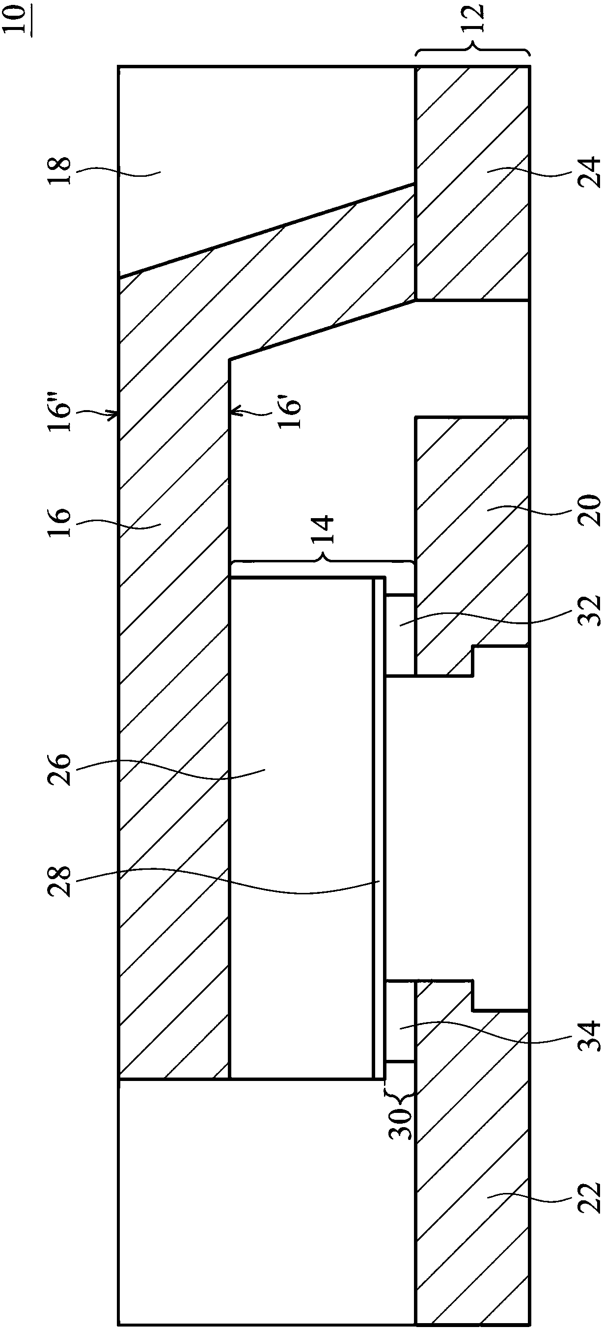
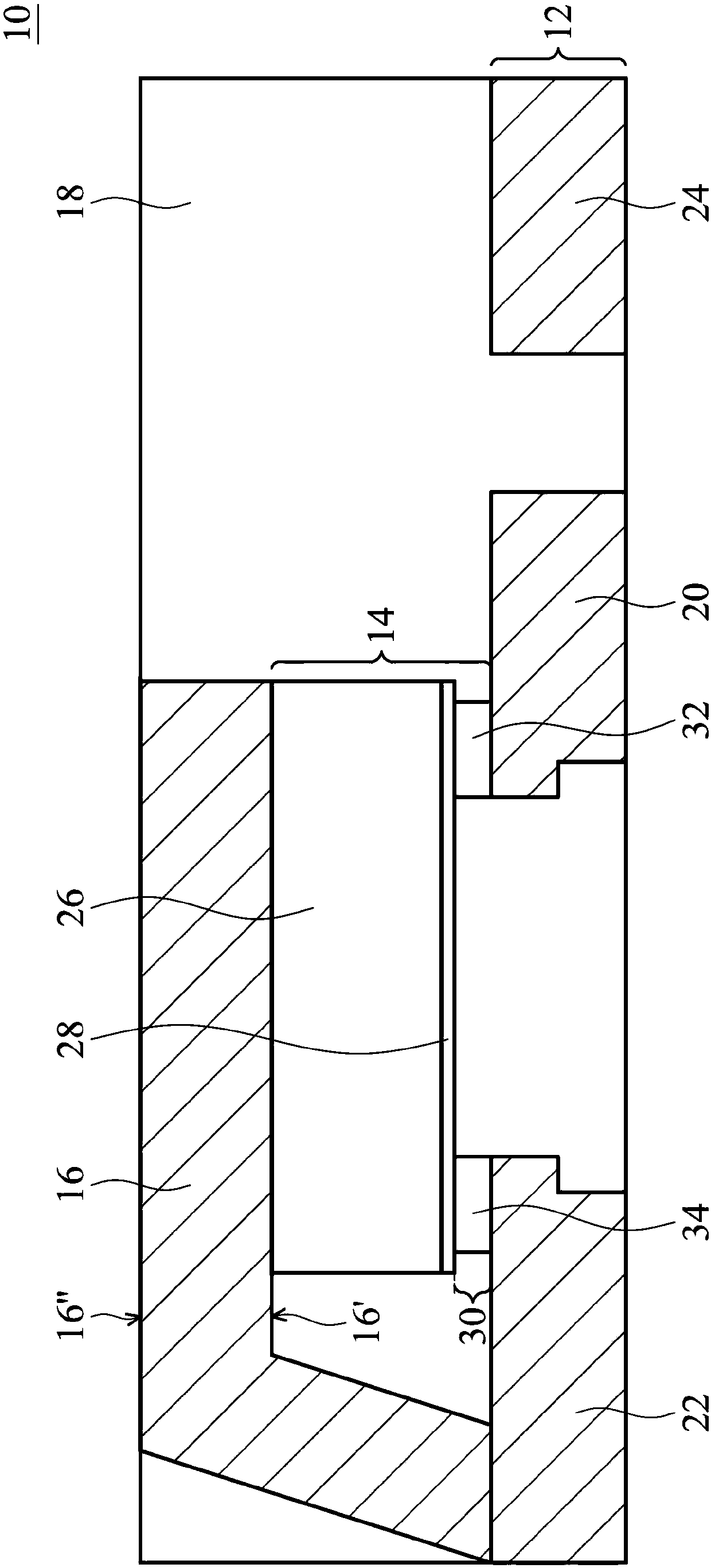
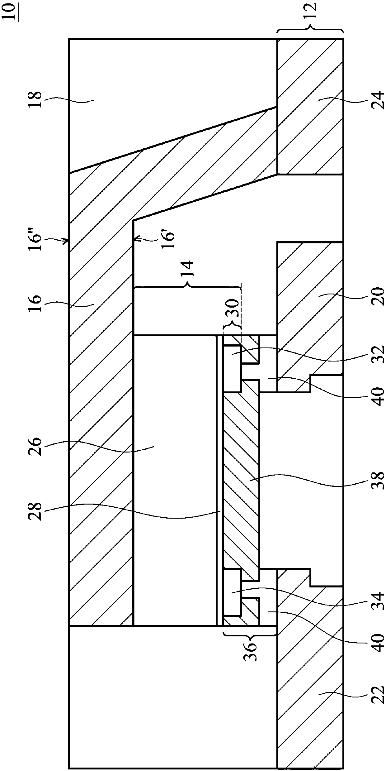
[0046] see figure 1 , according to an embodiment of the present disclosure, a package structure 10 is provided. figure 1 is a schematic cross-sectional view of the package structure 10 .

[0047] The packaging structure 10 includes a leadframe 12 , a device 14 , a conductive unit 16 , and a packaging material 18 . The lead frame 12 includes a plurality of connection parts, such as a first connection part 20 , a second connection part 22 , and a third connection part 24 . The device 14 includes a substrate 26 , an active layer 28 , and a plurality of electrodes 30 , such as a first electrode 32 and a second electrode 34 . The active layer 28 is disposed on the substrate 26 . The electrode 30 is disposed on the active layer 28 . It should be noted that the electrode 30 of the device 14 is connected to the connecting portion of the lead frame 12, for example, the first electrode 32 of the device 14 is connected to the first connecting portion 20 of the lead frame 12, and the ...


PUM

PropertyMeasurementUnit
lengthaaaaaaaaaa
diameteraaaaaaaaaa
heightaaaaaaaaaa

Abstract

A package structure is provided. The package structure includes a leadframe including a plurality of connection portions; a device including a substrate, an active layer disposed on the substrate anda plurality of electrodes disposed on the active layer, wherein the electrodes of the device are connected to the connection portions of the leadframe; a conductive unit having a first side and a second side, wherein the first side of the conductive unit connects to the substrate of the device and the conductive unit connects to at least one of the connection portions of the leadframe; and an encapsulation material covering the device and the leadframe, wherein the second side of the conductive unit is exposed from the encapsulation material.

Description

technical field [0001] The present disclosure relates to a package structure, in particular to a package structure with at least partially exposed conductive units. Background technique [0002] Flip chip packaging describes the method of electrically connecting a die to a package carrier. A package carrier, such as a substrate or leadframe, provides connections from the die to the outside of the package. In standard packaging processes, wires are used to form the interconnects between the die and the carrier. The die is attached to the carrier face up, and then the wires are first bonded to the die, then wrapped around and bonded to the carrier. Generally, the length of the wire is between 1-5 cm and the diameter is between 15-35 microns. [0003] In contrast, in flip-chip packaging, the interconnection between the die and the carrier is formed through conductive bumps placed directly on the surface of the die. Place the bumped die upside down so that the bumps are dire...

Claims


Application Information

Patent Timeline
Patent Type & Authority Applications(China)
IPC IPC(8): H01L23/495H01L23/31
CPCH01L23/3121H01L23/49517H01L23/49568H01L2924/181H01L24/13H01L24/16H01L24/37H01L24/73H01L2224/13124H01L2224/13147H01L2224/16245H01L2224/73255H01L2924/00014H01L23/3107H01L23/49524H01L23/49562H01L24/40H01L2224/37147H01L2224/40245H01L2924/13091H01L2924/13055H01L2924/00012H01L2224/84H01L2924/00H01L2224/0237H01L2224/0239H01L2924/01029H01L2924/0665H01L2924/1306H01L23/49551H01L23/49548H01L23/49575H01L23/49541
Inventor 蔡欣昌李芃昕
Owner DELTA ELECTRONICS INC
Learn More