Y branch waveguide structure based on polymer asymmetric ridge waveguide

A technology of waveguide structure and ridge waveguide, which is applied in light guides, optics, instruments, etc., can solve the problems of poor stability of inorganic materials, increasing the angle and length of branch waveguides, large light energy radiation loss, etc.

Inactive Publication Date: 2018-04-03
UNIV OF ELECTRONIC SCI & TECH OF CHINA
View PDF3 Cites 0 Cited by
  • Summary
  • Abstract
  • Description
  • Claims
  • Application Information

AI Technical Summary

Problems solved by technology

[0005] At present, the optical waveguide using Silicon-On-Insulator (SOI) matrix or inorganic materials, although the former has low static power consumption, simple manufacturing process, and strong restrictions on light, the latter has better electro-optical effects and nonlinear effects, but SOI materials have the defects of low nonlinear optical coefficient, high dielectric constant and large loss, while inorganic materials have poor stability and are difficult to manufacture.
[0006] From the structural point of view, the symmetrical ridge waveguide Y branch structure currently used has a large radiation loss of light energy. To reduce the loss, the angle and length of the branch waveguide must be increased, which contradicts the miniaturization and compactness of the device.

Method used


Image

  • Y branch waveguide structure based on polymer asymmetric ridge waveguide
  • Y branch waveguide structure based on polymer asymmetric ridge waveguide
  • Y branch waveguide structure based on polymer asymmetric ridge waveguide

Examples


Embodiment Construction

[0024] In order to facilitate a further understanding of the structure and method of the present invention, the present invention will be described in detail below in conjunction with an example of an M-Z electro-optic modulator.

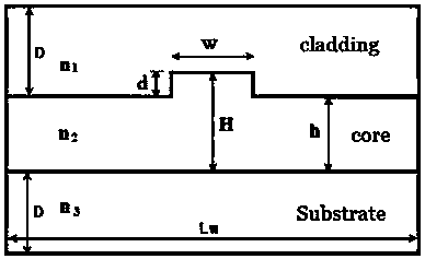
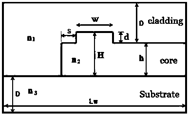
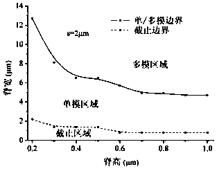
[0025] In this example, the waveguide core layer (core) material containing the ridge waveguide adopts IPC-E / polysulfone (n 2 =1.670), the upper cladding (cladding) material is NOA61 (n 1 =1.55), the lower cladding (substrate) material is UV15 (n 3 = 1.50). In order to ensure single-mode transmission, the parameters of the waveguide are: core layer thickness h = 1.5 μm, waveguide ridge height d = 0.6 μm, waveguide ridge width w = 4 μm, short core width s = 2 μm; upper cladding and lower The thickness of the cladding is D=6μm, and the width is L w = 40 μm. Symmetrically structured waveguide cross-sections such as figure 1 , the waveguide cross-section of the asymmetric structure is as figure 2 , the single-mode conditional curve such as imag...


PUM


Abstract

The invention relates to the optical integrated circuit field and discloses a Y branch waveguide structure based on a polymer asymmetric ridge waveguide. The Y branch waveguide structure based on thepolymer asymmetric ridge waveguide particularly targets a characteristic that an integrated optical waveguide is required to have a small volume and is applied to a curved waveguide in the Y branch waveguide in order to reduce radiation loss generated by the curved waveguide and reduce the length of the branch waveguide through adopting a structure that a flat plate core layer in the ridge waveguide is not asymmetric relative to the two sides of the ridges. The Y branch waveguide structure based on the polymer asymmetric ridge waveguide is characterized in that the curved waveguide adopts a ridge waveguide; widths of core layers on two sides of a ridge are not equal; and the core layer on the outside of the curved waveguide is pretty narrow (deep etching). The Y branch waveguide structurenot only can limit radiation loss of an optical field in the curved waveguide, but also can make a center of a guided mode of the optical field shifts to the middle of the waveguide. The Y branch waveguide structure based on the polymer asymmetric ridge waveguide is simple in structure, short in length and easy to implement. The Y branch waveguide structure based on the polymer asymmetric ridge waveguide shortens the size of the Y branch waveguide and provides an effective means to further miniaturizing an optical integrator.

Description

technical field [0001] The invention relates to the field of optical integrated circuits, in particular to an organic polymer-based Y-branch waveguide with an asymmetric ridge waveguide structure. The invention can be specifically applied to M-Z electro-optic modulators, optical power splitters and optical switches. Background technique [0002] With the rapid development of optical fiber communication networks, in order to achieve low-cost, high-performance optical transmission and high-speed optical link optical communication, not only higher requirements are put forward for high data transmission rates, but also for optical devices in optoelectronic equipment. requirements for further integration and miniaturization. [0003] As an important part of optical integrated devices such as power splitters, optical switches, and M-Z modulators, Y-branch waveguides are composed of straight waveguides and curved waveguides. After the modulated light is input from the input end o...

Claims


Application Information

Patent Timeline
IPC IPC(8): G02B6/125G02B6/122
CPCG02B6/125G02B6/1221
Inventor 高原杨昕梅李绍荣唐普英杨承
Owner UNIV OF ELECTRONIC SCI & TECH OF CHINA
Why Eureka
Try Eureka