
Self-aligning metal patterning based on photonic sintering of metal nanoparticles

A metal nanoparticle, nanoparticle technology, applied in nano-optics, nanotechnology for materials and surface science, nanotechnology, etc., can solve problems such as limited thickness, limited resolution, and reduced conductivity of metal films

Inactive Publication Date: 2018-03-27
NAT RES COUNCIL OF CANADA
View PDF7 Cites 1 Cited by
  • Summary
  • Abstract
  • Description
  • Claims
  • Application Information

AI Technical Summary

Problems solved by technology

However, there are serious drawbacks to using UV-curable metallic inks in self-aligned processes
First, UV-curable metallic inks contain photoinitiators and photocrosslinkers that remain in the film and reduce the conductivity of the resulting metallic film
Second, the printed metal film is opaque, and in this type of film, the depth of penetration of UV light is very limited, and the thickness that can be cross-linked is also very limited
Third, the resolution of the pattern completed by this ink is fundamentally limited by the size of its metal particles

Method used


Image

  • Self-aligning metal patterning based on photonic sintering of metal nanoparticles
  • Self-aligning metal patterning based on photonic sintering of metal nanoparticles
  • Self-aligning metal patterning based on photonic sintering of metal nanoparticles

Examples


Embodiment Construction

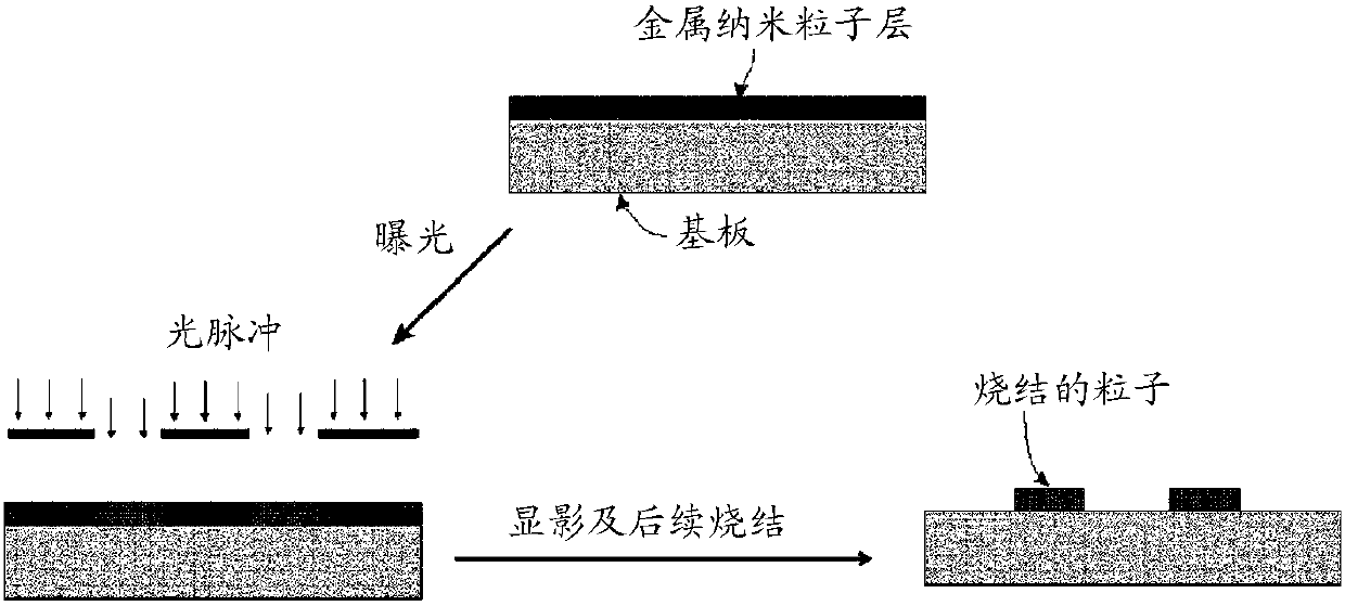
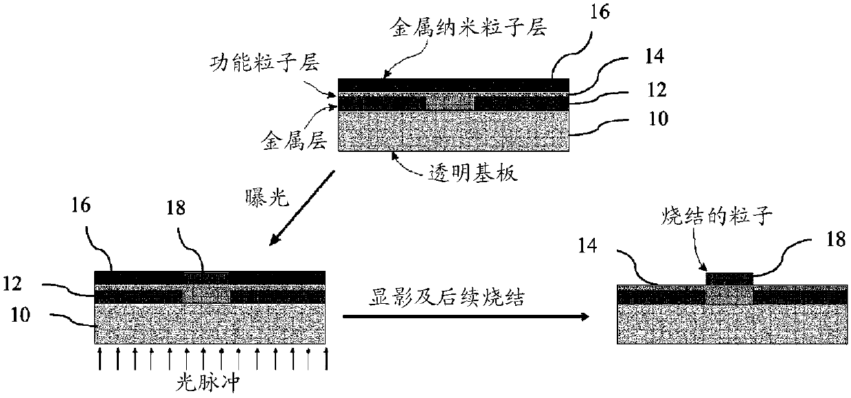
[0025] A method for self-aligned metal patterning using photonic sintering process and metal nanoparticle ink is disclosed herein. This approach avoids the need for multiple photolithography steps or vacuum deposition of metals. High-precision alignment of the upper layer to the underlying layer and the metal pattern between the lower layers is accomplished by using metal nanoparticle ink as a negative photoresist. The first metal layer printed on the transparent substrate acts as a mask to block light applied from the backside of the substrate. Intense pulses of light applied from the backside of the substrate partially sinter the exposed nanoparticles, ie those not covered by the mask. Masked metal nanoparticles are not affected by sintering and, therefore, can be washed away.

[0026] This method is primarily intended for use in the manufacture of electronic devices with multilayer structures by printing or equivalent low-cost deposition processes. Many electronic device...


PUM

PropertyMeasurementUnit
wavelengthaaaaaaaaaa
electrical resistanceaaaaaaaaaa
thicknessaaaaaaaaaa

Abstract

A method is disclosed for aligning layers in fabricating a multilayer printable electronic device. The method entails providing a transparent substrate upon which a first metal layer is deposited, providing a transparent functional layer over the first metal layer, depositing metal nano particles over the functional layer to form a second metal layer, exposing the metal nano particles to intense pulsed light via an underside of the substrate to partially sinter exposed particles to the functional layer whereby the first metal layer acts as a photo mask, and washing away unexposed particles using a solvent to leave partially sintered metal nano particles on the substrate.

Description

technical field [0001] The present disclosure relates generally to fabrication techniques for printable electronic devices, and more particularly to a technique for aligning layers in the fabrication of multilayer printable electronic devices. Background technique [0002] Printing functional inks on flexible, low-cost substrates is an increasingly popular method of manufacturing electronic devices. Multi-layer printing techniques, which are frequently used in the manufacture of electronic devices, remain challenging due to the difficulty in achieving the required accuracy of alignment or registration when upper layers are printed on top of lower layers. In order to solve the problem of layer-to-layer alignment accuracy, a self-alignment process (Palfinger et al, Adv. Mater. 2010, 22, 5115-5119) was proposed for printing organic transistors. In this method, the first metal layer is patterned by nanoimprint lithography or microcontact printing process, followed by a wet etch...

Claims


Application Information

Patent Timeline
Patent Type & Authority Applications(China)
IPC IPC(8): G03F7/00H01L29/772B82Y30/00H10K99/00
CPCG03F7/2022G03F7/40B82Y20/00G03F7/0043G03F7/2014G03F7/2016H10K10/464H10K10/466H10K71/611H10K71/621H10K77/10H10K2102/00B22F3/105B22F3/24B22F5/00B22F7/04B22F2003/247B22F2003/248B22F2301/052B22F2301/10B22F2301/255H05K1/097H05K3/06H05K3/064H05K3/4644H05K2201/0145H05K2203/013H05K2203/0548H05K2203/0766H05K2203/107H05K2203/1131
Inventor 张志一陶业朱达雅萧高志
Owner NAT RES COUNCIL OF CANADA
Learn More