CSP (Chip Scale Package) light source and manufacturing method and manufacturing die for same

A technology for manufacturing molds and light sources, applied in the field of lighting, can solve the problems of reduced luminous flux of light sources, separation of fluorescent colloids and light-emitting chips, insufficient brightness in the center of the light source, etc.

Inactive Publication Date: 2018-03-27
江西兆驰光元科技股份有限公司
View PDF7 Cites 1 Cited by
  • Summary
  • Abstract
  • Description
  • Claims
  • Application Information

AI Technical Summary

Problems solved by technology

[0005] (1) Since all five sides emit light, the center brightness of the light source is insufficient, so it cannot be applied to areas with high center brightness requirements such as mobile phone flashlights;
[0006] (2) The fluorescent glue on the bottom periphery of the light-emitting chip is excited by the blue light emitted by the light-emitting chip, and the light generated will be emitted from the lower part. This part of the light will usually be rapidly attenuated due to multiple refractions and reflections, resulting in the loss of the light source. The overall luminous flux is reduced, and the utilization rate of light is not high;
[0008] (4) Ordinary five-sided light-emitting CSP light source, the bonding of the light-emitting chip and the fluorescent colloid is based on the inherent adhesive properties of the colloid. This adhesive force is very small, making this CSP light source prone to fluorescence during use. The colloid is detached from the light-emitting chip, resulting in the failure of the light source

Method used


Image

  • CSP (Chip Scale Package) light source and manufacturing method and manufacturing die for same
  • CSP (Chip Scale Package) light source and manufacturing method and manufacturing die for same
  • CSP (Chip Scale Package) light source and manufacturing method and manufacturing die for same

Examples


Embodiment Construction

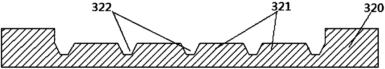
[0046] see Figure 3-5 , Embodiment 1 of the CSP light source of the present invention, which includes a light-emitting chip 210, a fluorescent colloid layer 220 is provided on the top of the light-emitting chip 210, and a light-reflective glue layer 230 with light-reflecting properties is surrounded around the light-emitting chip 210. The bonding part of the reflective adhesive layer 230 is an inclined structure, so that the fluorescent colloid layer 220 forms a structure with a large top and a small bottom, which can gather the light emitted by the flip chip on the top of the light source, such as Figure 5 As shown, the leakage of light from the bottom is well avoided, and the overall light extraction efficiency of the light source is improved.

[0047] In this embodiment, the junction of the fluorescent colloid layer 220 and the reflective adhesive layer 230 is a slope, the fluorescent colloid layer is an inverted trapezoid, and the intersection of the fluorescent colloid ...


PUM


Abstract

The invention provides a CSP (Chip Scale Package) light source and a manufacturing method and a manufacturing die for the same. The CSP light source comprises a light emitting chip; a fluorescent adhesive layer is arranged at the top of the light emitting chip; the periphery of the light emitting chip is surrounded with a reflective adhesive layer with reflection performance; a combining positionof the fluorescent adhesive layer and the reflective adhesive layer is of an inclined structure. Bosses and grooves are formed at intervals in a cavity of the manufacturing die for the CSP light source, which is provided by the invention. The manufacturing method for the CSP light source, which is provided by the invention, comprises the steps of: (1) fixing the light emitting chips on the bossesof the manufacturing die for the CSP light source; (2) coating a reflective adhesive between the light emitting chips and in the grooves and carrying out curing; (3) taking out a combined body of thelight emitting chips and the reflective adhesive and placing inversely; (4) full filling a fluorescent adhesive at a concave position of the combined body of the light emitting chips and the reflective adhesive and carrying out curing; and (5) cutting a cured module apart along the central axes of the adjacent light emitting chips to divide into single independent light sources. According to the invention, light emitted by a flip chip can be gathered at the top of the light source so as to well avoid leakage of the light from the bottom and promote integral light emergent efficiency of the light source.

Description

【Technical field】 [0001] The invention relates to the field of lighting, in particular to a CSP light source with high light extraction rate, a manufacturing method and a manufacturing mold thereof. 【Background technique】 [0002] The existing common five-sided light-emitting CSP light source (Chip Scale Package, chip scale package) structure is as follows figure 1 , figure 2 As shown, it consists of a light-emitting chip 110 in the middle and a fluorescent colloid 120 surrounding the light-emitting chip from above and around. Among them, the light-emitting chip 110 is a flip-chip with electrodes located at the bottom of the chip, so that the light source can be directly welded to the application end substrate, eliminating the need for a wire bonding process, and at the same time avoiding the reliability problem that the traditional SMD light source is easy to disconnect and die; the fluorescent glue is made of It is made by mixing transparent silica gel, fluorescent powd...

Claims


Application Information

Patent Timeline
IPC IPC(8): H01L33/50H01L33/54H01L33/56H01L33/60H01L21/56
CPCH01L21/565H01L33/505H01L33/54H01L33/56H01L33/60H01L2933/0041H01L2933/005H01L2933/0058
Inventor 周波何至年唐其勇
Owner 江西兆驰光元科技股份有限公司
Why Eureka
Try Eureka