Multi-layer PCB manufacturing method and multi-layer PCB

A production method and copper layer technology, applied in multilayer circuit manufacturing, printed circuit manufacturing, electrical components, etc., can solve the problem of low wiring density, achieve the effect of increasing wiring density and reducing the number of vias

Inactive Publication Date: 2018-03-23
DONGGUAN SHENGYI ELECTRONICS
View PDF4 Cites 4 Cited by
  • Summary
  • Abstract
  • Description
  • Claims
  • Application Information

AI Technical Summary

Problems solved by technology

[0003] The purpose of the present invention is to provide a method for making multilayer PCB and multilayer PCB, to overcome the defect of low product wiring density existing in the prior art

Method used


Image

  • Multi-layer PCB manufacturing method and multi-layer PCB
  • Multi-layer PCB manufacturing method and multi-layer PCB
  • Multi-layer PCB manufacturing method and multi-layer PCB

Examples


Embodiment Construction

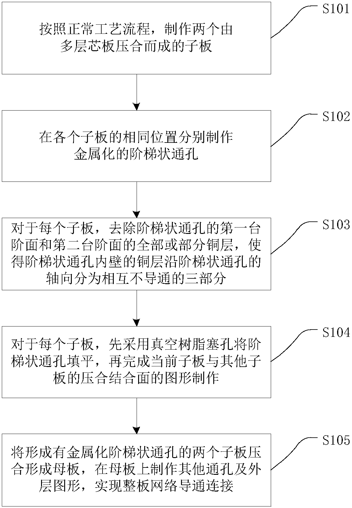
[0035] In order to make the purpose, features and advantages of the present invention more obvious and understandable, the technical solutions in the embodiments of the present invention will be clearly and completely described below in conjunction with the accompanying drawings in the embodiments of the present invention. Obviously, the following The described embodiments are only some, not all, embodiments of the present invention. Based on the embodiments of the present invention, all other embodiments obtained by persons of ordinary skill in the art without making creative efforts belong to the protection scope of the present invention.

[0036] see figure 1 , figure 1 The process flow of the manufacturing method of the multi-layer PCB is shown.

[0037] In the present embodiment, the manufacturing method of multilayer PCB comprises the following steps:

[0038] S101. According to the normal technological process, two sub-boards are manufactured respectively.

[0039] ...


PUM


Abstract

The invention discloses a multi-layer PCB manufacturing method and a multi-layer PCB. The manufacturing method comprises the steps that at least two sub-boards are manufactured and at least two sub-boards are pressed to form a mother board. The manufacturing method of the sub-boards comprises the steps that a stepped through hole is manufactured and metallized at the same position on each sub-board; each stepped through hole comprises a first through hole part with a large hole diameter and a second through hole part with a small hole diameter along the axial direction, and a first step surface is formed between the first through hole part and the second through hole part; entire or part of the copper layer of each first step surface is removed, so that the copper layer on the inner wall of each stepped through hole is disconnected to form two parts which are non-conducting; and when at least two sub-boards are pressed to form a mother board, the position of the stepped through hole ofeach sub-board is kept the same from top to bottom. According to the embodiment of the invention, the copper layer on the inner wall of the stepped through hole of each sub-board is divided into twoparts or three parts; when the sub-boards of all layer are pressed together to form the mother board, more network connection layers are realized at the position of the same hole in the mother board;the number of vias is greatly reduced; and the PCB wiring density is improved.

Description

technical field [0001] The invention relates to the technical field of PCB (Printed Circuit Board, printed circuit board), in particular to a method for manufacturing a multilayer PCB and the multilayer PCB. Background technique [0002] With the development of high-density integrated circuit technology and microelectronics technology, the volume of electronic products has become lighter, thinner and smaller. Traditional high-density designs usually use HDI technology, N+N technology, large and small hole technology, etc. to reduce the number of vias and increase wiring density. Among them, the HDI technology is complex and the product yield rate is low; the N+N technology and the large and small hole technology can only go through one hole and two lines, and the product wiring density is not high. Contents of the invention [0003] The object of the present invention is to provide a method for manufacturing a multilayer PCB and a multilayer PCB, which overcome the defect...

Claims


Application Information

Patent Timeline
IPC IPC(8): H05K3/46
CPCH05K3/4611H05K3/4614H05K2203/0214
Inventor 王小平何思良纪成光赵刚俊陈正清金侠
Owner DONGGUAN SHENGYI ELECTRONICS
Why Eureka
Try Eureka