Preparation method of photoelectric component

A technology of optoelectronic components and light, applied in the direction of electrical components, semiconductor/solid-state device manufacturing, circuits, etc.

Inactive Publication Date: 2018-03-13
DAXIN MATERIALS
View PDF9 Cites 0 Cited by
  • Summary
  • Abstract
  • Description
  • Claims
  • Application Information

AI Technical Summary

Problems solved by technology

The peeling layer in this patent announcement is peeled off by applying ultraviolet light or laser, and the materials of the peeling layer and the adhesive layer and the solvent used to remove the residue of the adhesive layer are not disclosed in detail.

Method used


Image

  • Preparation method of photoelectric component
  • Preparation method of photoelectric component
  • Preparation method of photoelectric component

Examples


Embodiment

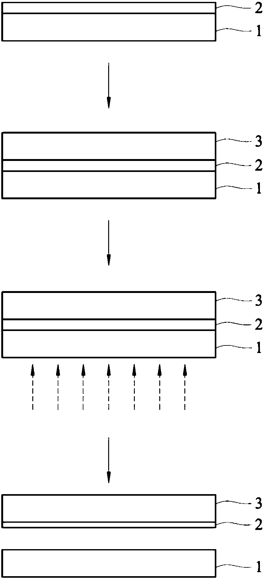
[0036] refer to figure 1 , the embodiment of the preparation method of the photoelectric element of the present invention comprises:

[0037] (a) Forming a polymer layer 2 on the carrier material 1, the polymer layer 2 is mainly a material that will degrade under light irradiation. In this embodiment, the polymer layer 2 is mainly made of polyimide material, and the polymer layer 2 is made by combining 2,2'-bis(trifluoromethyl)benzidine (TFMB) with 4, The polyimide formed by the reaction of 4'-oxydiphthalic anhydride (ODPA) and hexafluorodianhydride (6FDA) is coated on the glass carrier 1, and then heated at 300°C for dehydration and ring-closing reaction to form .

[0038] (b) forming a photoelectric element 3 on the polymer layer 2;

[0039] (c) irradiating the polymer layer 2 with light from the surface of the glass carrier, so that the polymer layer 2 is degraded, and the glass carrier 1 is separated from the photoelectric element 3; and

[0040] (d) Cleaning the optoele...


PUM

PropertyMeasurementUnit
Boiling pointaaaaaaaaaa
Thicknessaaaaaaaaaa

Abstract

The invention discloses a preparation method of a photoelectric component, which includes the steps of: a) forming a high-molecular layer on a base material, wherein the photoelectric component mainlyincludes a material which is degraded under light radiation; b) forming a photoelectric component above the photoelectric component; c) irradiating the high-molecular layer to degrade the high-molecular layer and separate the base material from the photoelectric component; d) using a cleaning composition to clean the base material or the photoelectric component, wherein the cleaning composition includes chain carbonate represented as the formula (1), and an organic solvent of which Hansen dissolubility parameter range is 9-15 (cal / cm<3>)1 / 2. The preparation method includes the step of cleaning the composition so that the high-molecular layer does not remain on the base material or the photoelectric component, and the base material is easy to recycle.

Description

technical field [0001] The invention relates to a method for preparing a photoelectric element, in particular to a method for preparing a photoelectric element that uses light irradiation to separate a carrier material (carrier) from the photoelectric element. Background technique [0002] In the fields of optoelectronics, electronics, and semiconductors, mostly multilayer thin film substrates (that is, integrated (integrated) circuit integrated substrates) are used to manufacture optoelectronic or semiconductor devices. With the increase in the number of functional optoelectronic components and the demand for miniaturization of optoelectronic devices, multilayer thin film substrates are also required to have high precision, and special dimensional stability must be maintained during the manufacturing process. In order to maintain good dimensional stability, the most commonly used improvement method at present is to manufacture multi-layer thin film substrates on a rigid car...

Claims


Application Information

Patent Timeline
IPC IPC(8): H01L21/56
CPCH01L21/568
Inventor 张灵卢厚德
Owner DAXIN MATERIALS
Why Eureka
Try Eureka