
A UWB Microstrip Vertical Transition Based on Single-Layer Microwave Dielectric

A microwave medium and vertical transition technology, applied in the electronic field, can solve the problems of inaccuracy and inapplicability, and achieve the effect of simplifying the process of process realization, high processing precision and excellent performance

Active Publication Date: 2020-04-10
XIAN INSTITUE OF SPACE RADIO TECH
View PDF4 Cites 0 Cited by
  • Summary
  • Abstract
  • Description
  • Claims
  • Application Information

AI Technical Summary

Problems solved by technology

Usually because its design requires microstrip multi-layer substrates, common single-layer substrates such as A493 ceramic dielectric substrates cannot use this method
Some multi-layer dielectric substrates have the problem of dielectric pressure and inaccurate alignment during sintering, such as LTCC substrates. If the transition structure is designed with LTCC, it cannot be applied to higher frequency bands due to its alignment error.

Method used


Image

  • A UWB Microstrip Vertical Transition Based on Single-Layer Microwave Dielectric
  • A UWB Microstrip Vertical Transition Based on Single-Layer Microwave Dielectric
  • A UWB Microstrip Vertical Transition Based on Single-Layer Microwave Dielectric

Examples


Embodiment 1

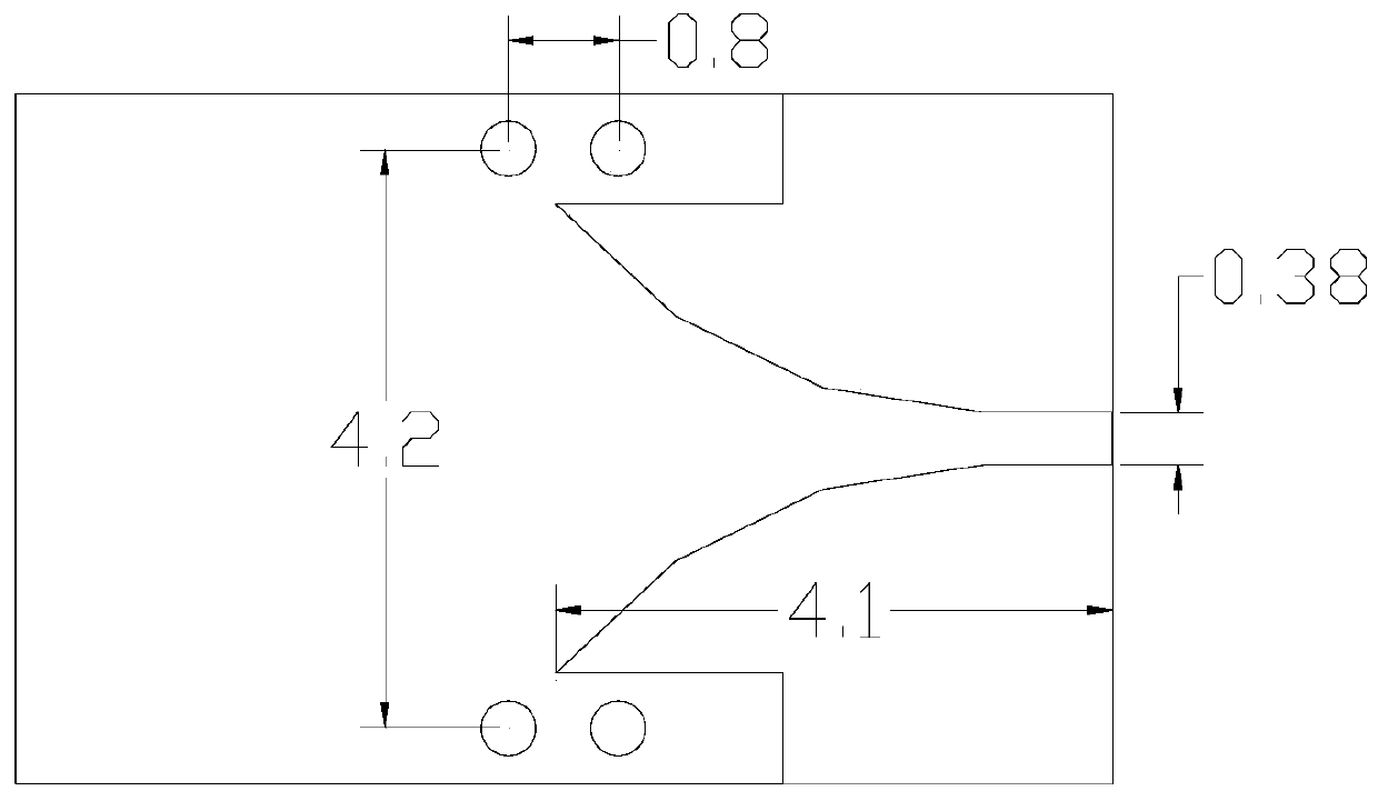
[0030] The present invention takes a microstrip vertical transition from X to Ka frequency band based on a single-layer ceramic medium as an example. Such as figure 2 As shown, the dielectric substrate material uses the ceramic substrate material A493, the relative dielectric constant is 9.9, and the dielectric thickness is 0.38mm.

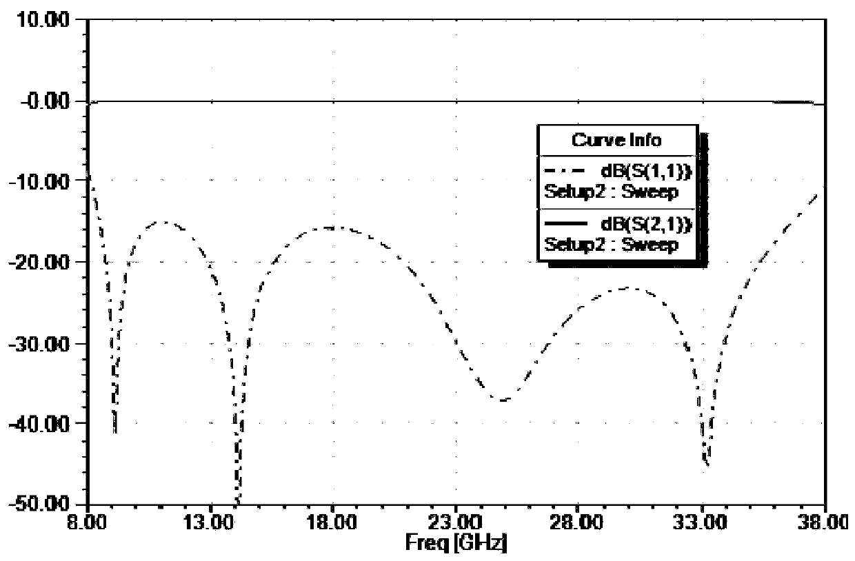
[0031] Its topology has been described in detail above, and its specific dimensions are as follows figure 2 shown. The simulation results of the new ultra-wideband high-frequency microstrip vertical transition in this example are as follows: image 3 As shown, dB(S(1,1)) is its reflection loss, and dB(S(2,1)) is its insertion loss. Its frequency band can cover 8GHz to 38GHz, and the bandwidth can reach 30GHz, and it can be easily improved by reducing the corresponding size. Use frequencies up to the mmWave band.

Embodiment 2

[0033] Such as Figure 4 As shown, the A493 ceramic medium is also used, and the thickness of the medium is 0.254mm. The simulation results are as follows Figure 5 As shown, dB(S(1,1)) is its reflection loss, and dB(S(2,1)) is its insertion loss, and its transmission performance can cover the entire frequency band from 18GHz to 50GHz.

[0034] In summary, the ultra-broadband high-frequency microstrip vertical transition method proposed by the present invention has simple implementation form, flexible design, high applicable frequency, wide applicable bandwidth, excellent standing wave in the band, and can be applied to various required radio frequency microwave system or circuit.


PUM

PropertyMeasurementUnit
thicknessaaaaaaaaaa
relative permittivityaaaaaaaaaa

Abstract

An ultra wide band micro-strip vertical transition based on a single layer microwave medium is based on the single layer medium substrate; an upper metal layer and a lower metal layer are employed; each layer comprises a 50 ohm microstrip line, a non-linear transition coupling line, a ground plane, rectangular area branches, and a metallization grounding hole; the 50 ohm microstrip line transits to the ground plane through the non-linear transition coupling line; the rectangular area branches extend out from the ground plane, located on two sides of the non-linear transition coupling line, andprovided with the metallization grounding hole so as to connected with the other layer of rectangular area branch or the ground plane. The vertical transition based on the single layer microwave medium substrate employs the method by which the microstrip quasi-TEM mode transits to the microstrip coupling structure and transits to the quasi-TEM mode; the upper and lower microstrip structures are symmetrically arranged with respect to the center; the process is easy to realize; the vertical transition is high in usage frequency, can be applied to the Ka frequency range and the millimeter wave frequency range, is wide in work bandwidth, and the relative bandwidth approaches to the 1.5 times of octave.

Description

technical field [0001] The invention relates to an ultra-broadband microstrip vertical transition based on a single-layer microwave medium, which belongs to the field of electronic technology. Background technique [0002] In the design of microwave radio frequency and millimeter wave stand-alone, it is often encountered that the microwave signal needs to be transmitted from one side of the cavity to the other side of the cavity, or in multilayer microwave dielectric substrates such as LTCC and RO4003C, it is necessary to transfer the microwave signal from the substrate to the other side of the cavity. transfer from one layer to another. [0003] There are usually two methods for the vertical transition of the microstrip: 1. The vertical transmission transition of the microstrip line is realized based on the metal via. However, since the metal via is equivalent to a series inductance, it has a low-pass characteristic. As the frequency increases, this type of vertical trans...

Claims


Application Information

Patent Timeline
Patent Type & Authority Patents(China)
IPC IPC(8): H01P3/18
CPCH01P3/18
Inventor 李斌陈钚王国瑾于长龙姚欣段西航
Owner XIAN INSTITUE OF SPACE RADIO TECH
Learn More