
Chucks, reaction chambers and semiconductor processing equipment

A chuck and body technology, which is applied in the fields of chucks, reaction chambers and semiconductor processing equipment, can solve the problems of inability to meet the rapid cooling of the wafer, limited contact area, high temperature damage of the wafer, etc., so as to improve the cooling effect and increase the contact area. , to avoid the effect of high temperature damage

Active Publication Date: 2021-09-17
BEIJING NAURA MICROELECTRONICS EQUIP CO LTD
View PDF6 Cites 0 Cited by
  • Summary
  • Abstract
  • Description
  • Claims
  • Application Information

AI Technical Summary

Problems solved by technology

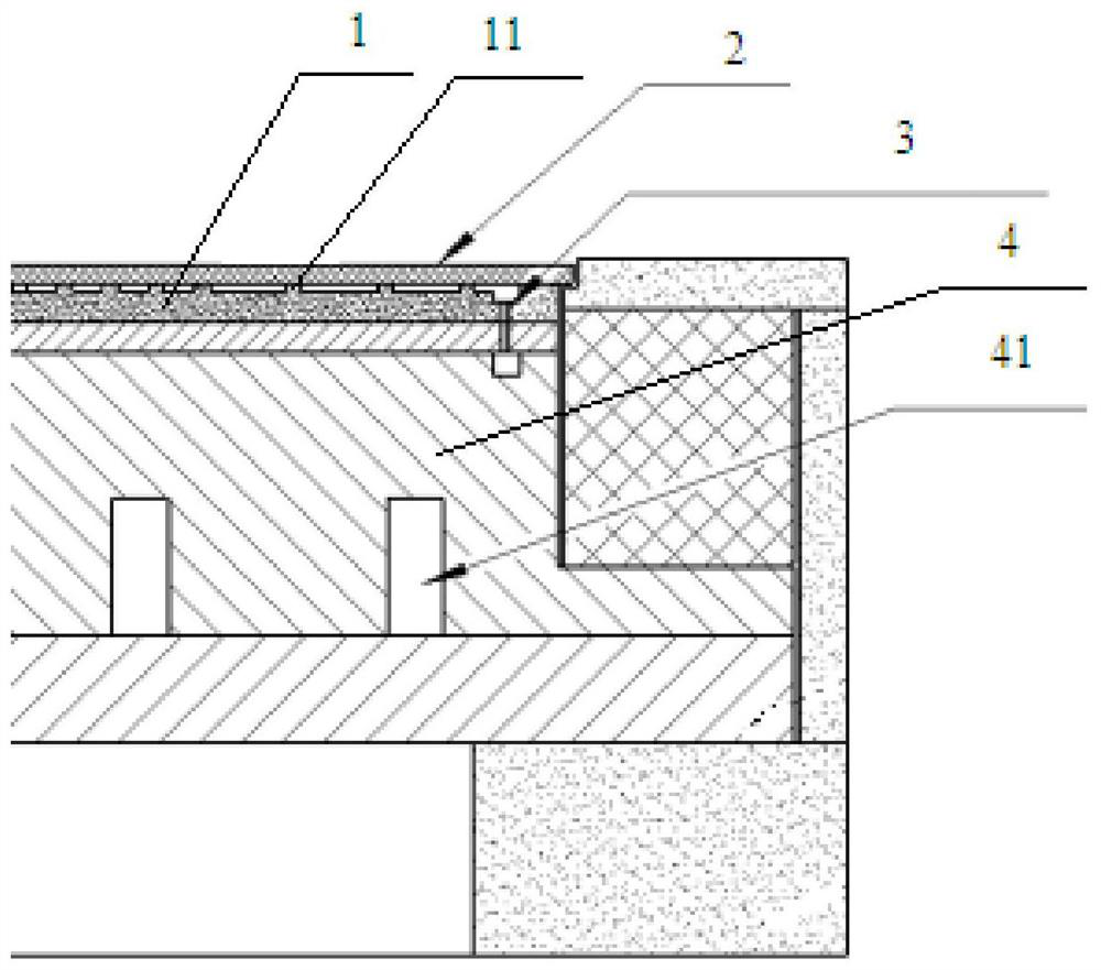
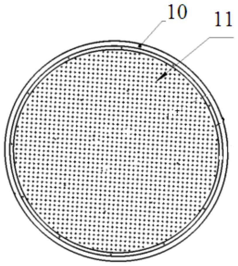
[0006] The heat transfer between the insulating layer 1 and the wafer 2 mainly relies on the contact of a plurality of bumps 11 with the lower surface of the wafer 2, and the cooling gas between the insulating layer 1 and the wafer 2, but, due to the contact between the bumps 11 and the wafer 2 The lower surface is in point contact, and the contact area is limited, which cannot meet the needs of rapid cooling of the wafer, especially when the high-temperature process is performed, the surface temperature of the wafer rises rapidly, resulting in high-temperature damage to the wafer

Method used


Image

  • Chucks, reaction chambers and semiconductor processing equipment
  • Chucks, reaction chambers and semiconductor processing equipment
  • Chucks, reaction chambers and semiconductor processing equipment

Examples


Embodiment Construction

[0030] In order for those skilled in the art to better understand the technical solution of the present invention, the chuck, the reaction chamber and the semiconductor processing equipment provided by the present invention will be described in detail below with reference to the accompanying drawings.

[0031] image 3 A cross-sectional view of the chuck provided by the embodiment of the present invention. Figure 4 for image 3 Zoom-in view of the middle I region. Please also refer to image 3 and Figure 4 , the chuck includes a body and a base 7, wherein the body includes a first carrying surface 51 and a second carrying surface 52 surrounding the periphery of the first carrying surface 51, the first carrying surface 51 is used to carry the central area of ​​the wafer 6, The second carrier surface 52 is used for carrier of the edge region of the wafer 6 . Wherein, the first carrying surface 51 has a first roughness, and the first roughness can increase the thickness of...


PUM


Abstract

The invention provides a chuck, a reaction chamber and semiconductor processing equipment. The chuck of the present invention includes a body and a base body. The body includes a first carrying surface and a second carrying surface surrounding the outer periphery of the first carrying surface. The first carrying surface is used for carrying the central area of ​​the wafer, and the second carrying surface is used for carrying The edge region of the wafer, wherein the first carrying surface has a first roughness, and the first roughness can increase the gap between the wafer and the first carrying surface under the premise of ensuring that the gas located between the first carrying surface and the wafer is evenly distributed. the contact area between them. The reaction chamber of the invention comprises the chuck of the invention. The semiconductor processing equipment of the present invention includes the reaction chamber of the present invention. The chuck provided by the invention can improve the efficiency of heat conduction from the wafer to the chuck, and avoid damage caused by excessively fast temperature rise on the wafer surface.

Description

technical field [0001] The invention relates to the field of semiconductor manufacturing, in particular to a chuck, a reaction chamber and semiconductor processing equipment. Background technique [0002] Electrostatic Chuck (ESC) is widely used in the manufacturing process of integrated circuits, especially plasma etching (ETCH), physical vapor deposition (PVD), chemical vapor deposition (CVD) and other processes. ESC is required to fix the wafer in the reaction chamber, provide DC bias voltage for the wafer, and rapidly cool the wafer surface, so that the high temperature generated on the wafer surface during the process can be effectively controlled. [0003] figure 1 It is a partial sectional view of an existing electrostatic chuck. see figure 1 , the electrostatic chuck includes an insulating layer 1 and an aluminum base 4 for supporting the insulating layer 1 , wherein the upper surface of the insulating layer 1 is manufactured by ceramic material or ceramic sprayin...

Claims


Application Information

Patent Timeline
Patent Type & Authority Patents(China)
IPC IPC(8): H01L21/687H01L21/67
CPCH01L21/67207H01L21/67213H01L21/687H01J37/20H01J37/32H01L21/683
Inventor 张虎威
Owner BEIJING NAURA MICROELECTRONICS EQUIP CO LTD
Learn More