Negative sheet PCB tin spraying process

A technology of PCB board and negative film, which is applied in the field of tin spraying technology of negative PCB board, can solve the problems of tin accumulation process of negative PCB board tin spraying, etc., and achieve the effect of convenient operation, simple process method and prevention of tin accumulation

Active Publication Date: 2018-02-09
DIGITAL PRINTED CIRCUIT BOARD CO LTD
View PDF3 Cites 2 Cited by
  • Summary
  • Abstract
  • Description
  • Claims
  • Application Information

AI Technical Summary

Problems solved by technology

[0007] Based on this, it is necessary to address the existing technical problems and provide a negative PCB board tin spraying process, which

Method used


Image

  • Negative sheet PCB tin spraying process
  • Negative sheet PCB tin spraying process

Examples


Embodiment Construction

[0037] In order to further understand the features, technical means, and specific objectives and functions achieved by the present invention, the present invention will be further described in detail below in conjunction with the accompanying drawings and specific embodiments.

[0038] refer to Figure 1 to Figure 2 .

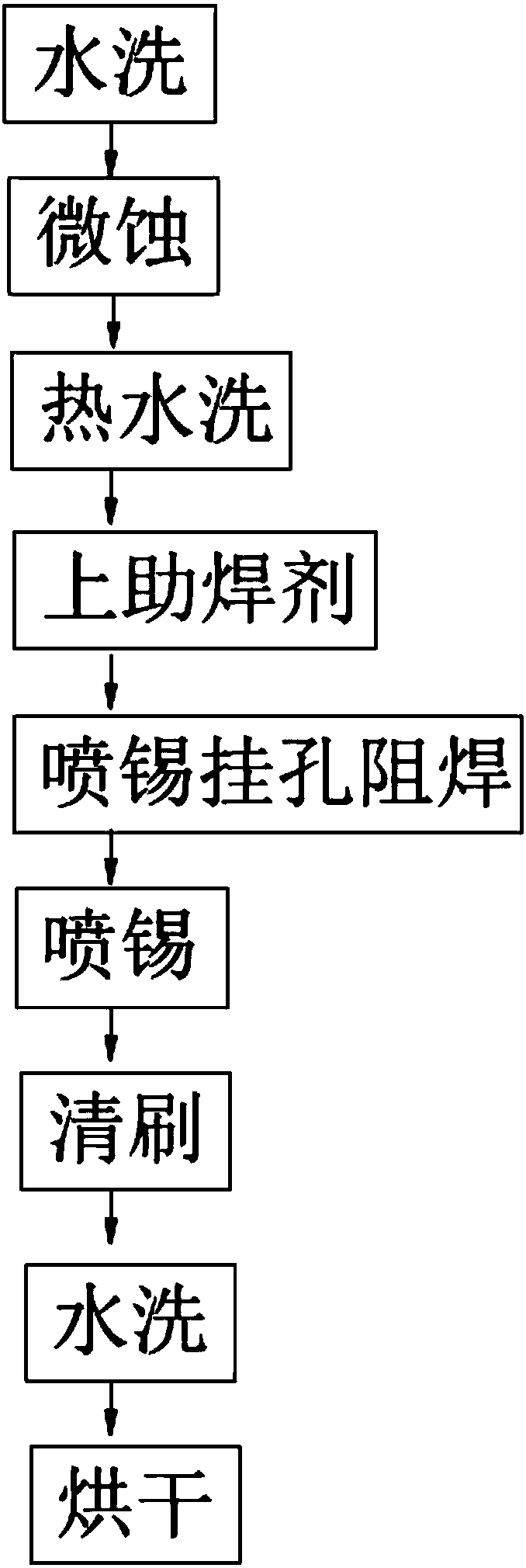
[0039] The embodiment of the present invention discloses a process of spraying tin on a negative PCB board, which includes the following steps:

[0040] A. Washing: wash and clean the PCB board;

[0041] B. Micro-etching: Micro-etch the PCB board to remove the outer copper surface, remove oil stains, and form a certain roughness on the surface of the PCB board;

[0042] C. Hot water washing: Clean the PCB board with hot water to remove residual substances on the surface of the PCB board;

[0043] D. Apply flux: apply flux to the surface of the PCB board to improve the soldering ability;

[0044] E. Solder resistance of the tin-sprayed hanging hole: apply so...


PUM

PropertyMeasurementUnit
Thicknessaaaaaaaaaa

Abstract

The invention provides a negative sheet PCB tin spraying process. The process comprises the following steps of A performing water washing; B performing micro etching; C performing hot water washing; Dusing soldering flux; E performing solder resisting on tin-sprayed suspension holes; F performing tin spraying; G performing cleaning and brushing; H performing water washing; and I performing drying. According to the negative sheet PCB tin spraying process, a measure of solder resisting is performed on the tin-sprayed suspension holes before tin spraying; the position of the tin-sprayed suspension holes is coated with solder resisting printing oil, and the printing oil is subjected to exposure, developing and baking to form a layer of solder resisting layer, so that the problem of tin accumulation in the position of the tin-sprayed suspension holes caused by the fact that the tin material is cured in the tin-sprayed suspension holes in the tin spraying operation can be prevented; the printing oil forms the solder resisting layer in the tin-sprayed suspension holes, so that tin material attachment in the tin-sprayed suspension holes in tin spraying can be avoided, and the tin-sprayedsuspension holes are tidy and leveled; a smooth, uniform and bright solder coating layer is obtained around the position of the tin-sprayed suspension holes; the process is simple in method, convenient to operate and capable of effectively preventing tin accumulation in the position of the tin-sprayed suspension holes; and the positions of the tin-sprayed suspension holes are tidy and uniform.

Description

technical field [0001] The invention relates to the technical field of PCB boards, and specifically discloses a tin-spraying process for a negative PCB board. Background technique [0002] At present, with the development of the electronics industry, PCB boards, as important electronic components, have been widely used. Negative film board is an important means of PCB board manufacturing. After the negative film board is produced, the required lines or copper surfaces are transparent, while the unnecessary parts are black or brown. After exposure through the circuit process, the transparent parts are dry The film resist is chemically hardened by light, and the subsequent development process will wash away the unhardened dry film, so that only the copper foil of the dry film protection part is bitten in the etching process, while the copper foil required for tin plating remains. After stripping the tin, the required lines are left. [0003] In the process of making PCB boar...

Claims


Application Information

Patent Timeline
IPC IPC(8): H05K3/34
CPCH05K3/34
Inventor 张文平
Owner DIGITAL PRINTED CIRCUIT BOARD CO LTD
Why Eureka
Try Eureka