A resistive memory for avoiding misreading and its preparation method
A resistive variable memory and resistive variable technology, applied in the direction of electrical components, etc., can solve the problems of switching voltage dispersion, poor uniformity and stability, and high power consumption, and achieve improved uniformity, good stability and uniformity, and low power consumption Effect
- Summary
- Abstract
- Description
- Claims
- Application Information
AI Technical Summary
Problems solved by technology
Method used
Image

Examples
Embodiment 1
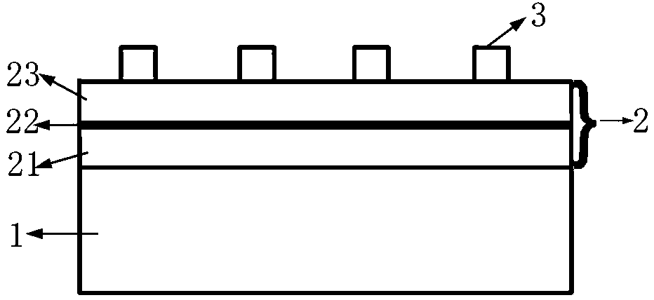
[0032] like figure 1 As mentioned above, the resistive memory for avoiding misreading provided by the present invention has a structure including Pt / Ti / SiO from bottom to top 2 / Si substrate 1, in Pt / Ti / SiO 2 The resistive variable medium layer 2 formed on the Pt film layer of the Si substrate 1 and the Ag electrode layer 3 formed on the resistive variable medium layer 2 . The resistive variable dielectric layer 2 includes a first zirconium hafnium oxide film layer 21 , a graphene oxide quantum dot intermediate layer 22 and a second zirconium hafnium oxide film layer 23 from bottom to top.
[0033] The thickness of the resistive medium layer 2 is 10~20nm, and the thickness of the graphene oxide quantum dot intermediate layer 22 is 0.8~1.2nm, preferably 1nm; the first zirconium hafnium oxide film layer 21 and the second zirconium hafnium oxide film layer The thickness of layer 23 is preferably the same.
[0034] The thickness of the Ag electrode layer is 50-200nm.
[0035] ...
Embodiment 2
[0045] (1) Pt / Ti / SiO 2 / Si substrate 1 is placed in a beaker filled with acetone, cleaned by ultrasonic waves for 10 minutes, then placed in a beaker filled with alcohol and cleaned by ultrasonic waves for 10 minutes, then taken out with clips and placed in a beaker filled with deionized water for ultrasonic cleaning 5min, then take it out and use nitrogen (N 2 ) and blow dry.
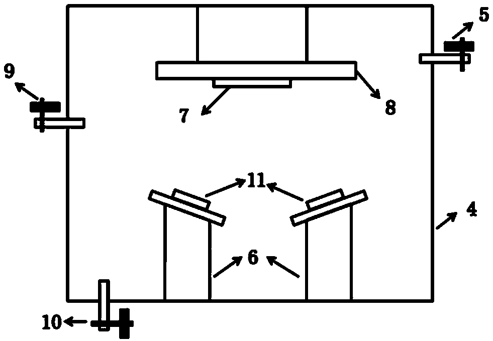
[0046] (2) Open the cavity 4 of the magnetron sputtering equipment, take out the tablet press table 7, first polish it with sandpaper until it shines, clean the organic matter attached to the surface of the tablet press table with acetone, and finally wipe it clean with alcohol; Pt / Ti / SiO 2 / Si substrate 1 is placed on the table 7 for tableting, and the Pt / Ti / SiO is ensured during tableting 2 / Si substrate 1 is firmly pressed on the tablet press table 7 and flattened to ensure uniform film growth during sputtering. After the tablet press is completed, it is placed on the substrate table 8 in the cav...
Embodiment 3
[0056] Example 3 Testing the performance of the resistive memory devices prepared by the present invention and comparative examples
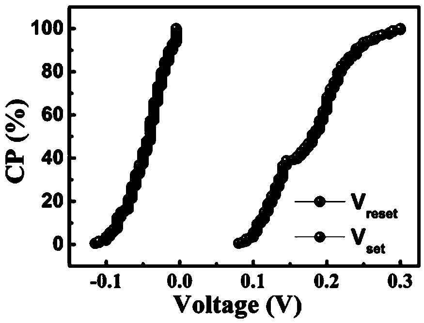
[0057] (1) 200 circles of current and voltage scans were performed on the RRAM prepared in Example 2 of the present invention and the RRAM prepared in Comparative Example 1, and the cumulative probability distribution of the on-on and off voltages was counted. The results are as follows image 3 (the present invention) and Figure 4 (Comparative Example 1), from image 3 It can be seen from the figure that the turn-on voltage of the device, that is, the set voltage, is distributed between 0.08V and 0.3V, most of which are mainly distributed between 0.15V and 0.2V; image 3 It can be seen that the shutdown voltage, that is, the reset voltage, is distributed between -0.14V~-0.01V, and most of them are mainly distributed between -0.05V~-0.1V. from Figure 4 It can be seen that the turn-on voltage of the device is distributed between 0.08V and 1....
PUM
| Property | Measurement | Unit |
|---|---|---|
| thickness | aaaaa | aaaaa |
| thickness | aaaaa | aaaaa |
| thickness | aaaaa | aaaaa |
Abstract
Description
Claims
Application Information
 - R&D
- Intellectual Property
- Life Sciences
- Materials
- Tech Scout
- Unparalleled Data Quality
- Higher Quality Content
- 60% Fewer Hallucinations
Browse by: Latest US Patents, China's latest patents, Technical Efficacy Thesaurus, Application Domain, Technology Topic, Popular Technical Reports.
© 2025 PatSnap. All rights reserved.Legal|Privacy policy|Modern Slavery Act Transparency Statement|Sitemap|About US| Contact US: help@patsnap.com