Electrical device, memory device, and semiconductor integrated circuit
A technology of storage devices and electrical components, applied in the direction of electrical components, semiconductor devices, circuits, etc.
- Summary
- Abstract
- Description
- Claims
- Application Information
AI Technical Summary
Problems solved by technology
Method used
Image

Examples
no. 1 example
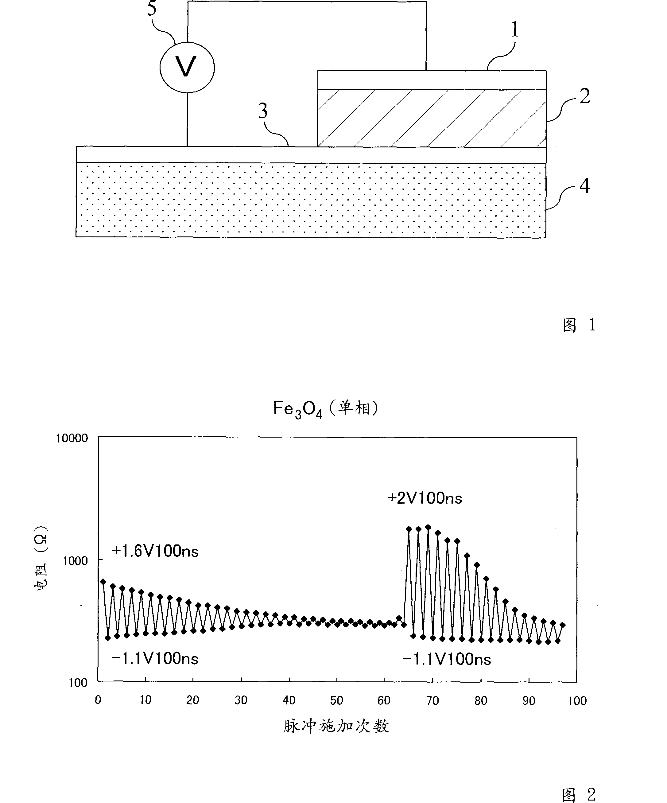
The electric element of the first embodiment of the present invention will be described below. And, as shown in FIG. 9, the circuit symbols of the electric elements used in this embodiment are defined. In FIG. 9, the upper electrode 1 of FIG. 1 is connected to a terminal 101-1. On the other hand, the lower electrode 3 of FIG. 1 is connected to the terminal 101-2.
[0069] As shown in FIG. 10 , when an electric pulse (positive polarity pulse) of "positive polarity" is applied to the electric element 102 with respect to the terminals 101-2 and 101-1, the resistance value of the electric element 102 decreases. Conversely, when an electric pulse (negative polarity pulse) of "negative polarity" is applied to the electric element 102 with respect to the terminals 101-2 and 101-1, the resistance of the electric element 102 increases. In other words, when an electric pulse is applied by causing a current to flow in the direction of the arrow, the resistance of the electric element...
no. 2 example
FIG. 12 shows the overall structure of a storage device 200 according to the second embodiment of the present invention. This device 200 has a memory array 201 , an address buffer 202 , a control unit 203 , a row decoder 204 , a word line driver 205 , a column decoder 206 , and a bit line / plate line driver 207 .
[0079] The memory array 201 is provided with word lines W1, W2, bit lines B1, B2, plate lines P1, P2, transistors T211, T212, T221, T222, and memory cells MC211, MC212, MC221, MC222. Memory cells MC211 to MC222 are electrical elements 102 shown in FIG. 9 .
[0080] The connection relationship between the transistors T211 to T222 and the memory cells MC211 to MC222 is the same, and the connection relationship between the transistor T211 and the memory cell MC211 will be described as a representative. The transistor T211 and the memory cell MC211 are connected in series between the bit line B1 and the plate line P1. Transistor T211 is connected between bit line B1 ...
no. 3 example
[0118]
[0119] [Write processing]
[0120] The logic circuit 301 outputs a mode selection signal MODE indicating "storage mode" to the control unit 203 of the memory circuit 200 in order to write predetermined data (for example, encrypted moving image data) into the memory device 200 .
[0121] Next, the logic circuit 301 sequentially outputs an address signal ADDRESS to the address buffer 202 of the memory device 200 in order to select a memory cell in which the predetermined data is to be written. Thus, in the memory device 200, the memory cells corresponding to the address signal ADDRESS are sequentially selected.
[0122] Next, the logic circuit 301 outputs the predetermined data of 1 bit each to the control unit 203 of the storage device 200 as 1-bit data Din.
[0123] Next, in the storage device 200, the same operations as in the storage mode of the second embodiment are performed. As a result, the predetermined data is written into the storage device 200 by 1 bit e...
PUM
 Abstract
Description
Claims
Application Information
 - R&D
- Intellectual Property
- Life Sciences
- Materials
- Tech Scout
- Unparalleled Data Quality
- Higher Quality Content
- 60% Fewer Hallucinations
Browse by: Latest US Patents, China's latest patents, Technical Efficacy Thesaurus, Application Domain, Technology Topic, Popular Technical Reports.
© 2025 PatSnap. All rights reserved.Legal|Privacy policy|Modern Slavery Act Transparency Statement|Sitemap|About US| Contact US: help@patsnap.com