
Laser two-beam interference photoetching system

A dual-beam interference and lithography system technology, which is applied in the field of laser dual-beam interference lithography systems, can solve problems such as limited production area, long process cycle, and restrictions on the exploration and research of new micro-nano prototype devices.

Inactive Publication Date: 2018-01-30
INST OF OPTICS & ELECTRONICS - CHINESE ACAD OF SCI
View PDF6 Cites 13 Cited by
  • Summary
  • Abstract
  • Description
  • Claims
  • Application Information

AI Technical Summary

Problems solved by technology

However, the above-mentioned post-lithography technology has problems such as the need for harsh environmental conditions such as vacuum, expensive equipment, low efficiency, long process cycle, and limited production area, which severely limits the exploration and research of new micro-nano prototype devices.

Method used


Image

  • Laser two-beam interference photoetching system
  • Laser two-beam interference photoetching system
  • Laser two-beam interference photoetching system

Examples


Embodiment 1

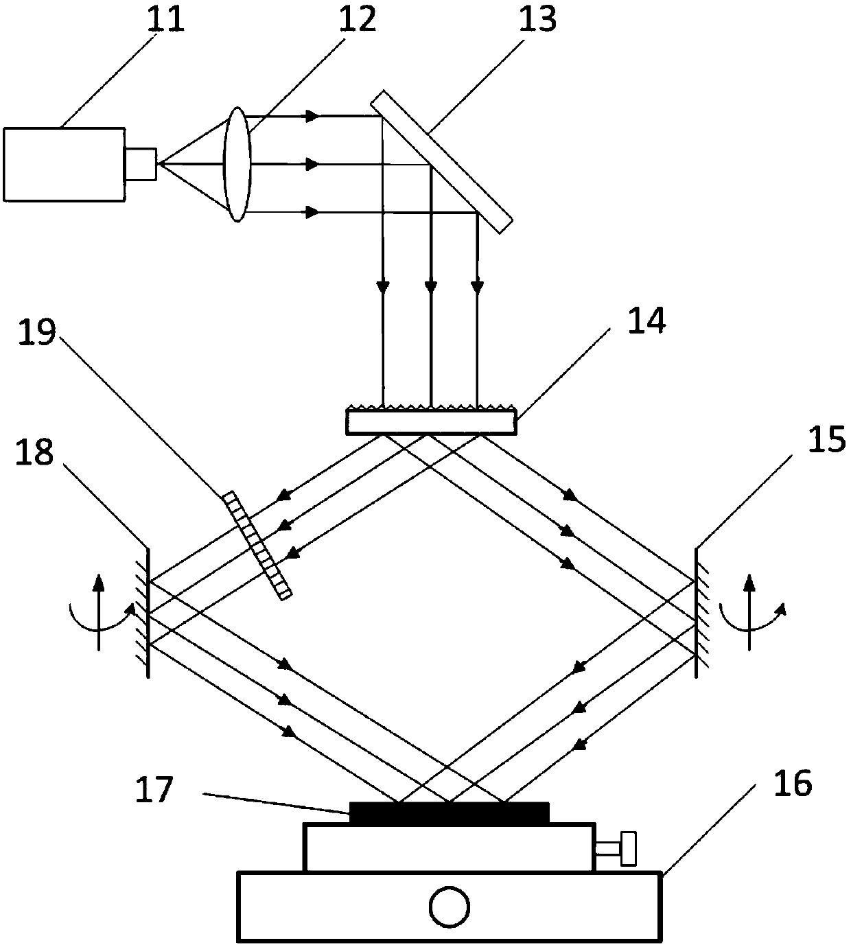
[0029] see figure 1 , is the optical path diagram of the laser double-beam interference lithography system disclosed in Embodiment 1 of the present invention. Such as figure 1 As shown, the system includes a He-cd laser 11, a collimating lens 12, a digital micromirror device (DMD) 13, a beam splitting grating 14, a first mirror 15, a 6-dimensional moving platform 16, a substrate 17, and a second mirror 18 and a spatial light modulator (SLM) 19, the collimating lens 12 collimates the laser beam from the He-cd laser 11 into parallel light, and the beam splitting grating 14 divides the incident laser light into two beams of light as a beam splitting element, and one beam is used as a reference beam , one beam enters the spatial light modulator 19 as modulated light, and interferes on the surface of the substrate 17 . The digital micromirror device (DMD) 13 and the spatial light modulator (SLM) 19 are directly controlled by a computer, so as to modulate the intensity and orienta...

Embodiment 2

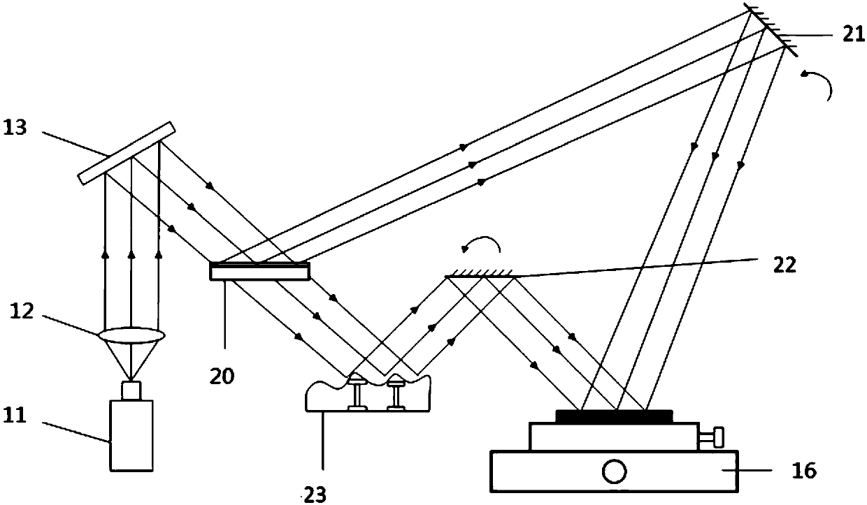
[0036] see figure 2 , is the optical path diagram of the laser double-beam interference lithography system disclosed in Embodiment 2 of the present invention, including a He-cd laser 11, a collimating lens 12, a digital micromirror device (DMD) 13, a half mirror 20, and a third reflector The mirror 21, the 6-dimensional moving platform 16, the fourth mirror 22 and the deformable mirror 23; in essence, the spatial light modulator is replaced by the deformable mirror as a phase modulation device. Other structural principles are the same as the first embodiment.


PUM


Abstract

The invention discloses a laser two-beam interference photoetching system. A laser field modulation technology is combined to realize the quick nanoscale processing of a large-area diversified periodic structure and a complex structure through one-time exposure or multi-time exposure. The system comprises that: a digital micromirror element is used for realizing ray gating, one path of incident light phase is modulated by a spatial light modulator or a deformable mirror to control the incidence space angle of modulation light and reference light, the regulation freedom degree and the range ofan interference beam angle of incidence are greatly increased, and a basis is provided for obtaining the diversity of an interference pattern. Through the two-beam interference photoetching system disclosed by the invention, a periodic or complex-structure large-area quick nanostructure is prepared on photoresist.

Description

technical field [0001] The invention belongs to the technical field of interference lithography, and in particular relates to a laser double-beam interference lithography system. Background technique [0002] The miniaturization and diversification of nano-devices is an important development direction of nanotechnology. Photolithography technology plays a leading role in the preparation of nano-devices. Photolithography technology is also developing towards the direction of large-area, rapid processing capability and complex structure preparation. . [0003] The principle of interference lithography technology is to use double-beam or multi-beam interference effect to produce light and dark stripes on the photoresist layer, and transfer the pattern generated by the interference to the substrate surface through a series of processes such as development. Its characteristic is that it does not need a mask, directly acts on the surface of the substrate, is easy to operate, and ...

Claims


Application Information

Patent Timeline
Patent Type & Authority Applications(China)
IPC IPC(8): G03F7/20G02B26/08
Inventor 严伟高洪涛田鹏李凡星彭伏平刘俊伯何渝杨帆吴云飞
Owner INST OF OPTICS & ELECTRONICS - CHINESE ACAD OF SCI
Learn More