


Quick Research
Generate reliable direction feasibility study reports for your R&D in just a few steps.

Technical Q&A
Discover and master advanced knowledge NOW. Basics, ideas, possibilities, all at once.

Find Solutions
As an expert in R&D theories, this can generate solutions to your technical problems instantly.

Evaluate Feasibility
Analyze your overall solution with one click, know your potential R&D risks in advance.

Monitor Landscape
Get weekly tech updates, stay abreast of the latest tech innovations and key insights.
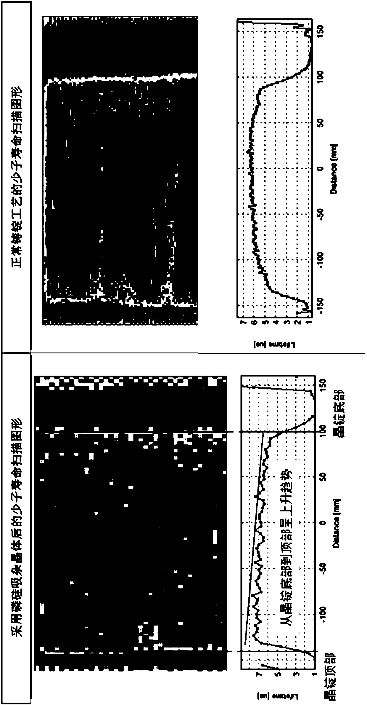
Method for increasing minority carrier lifetime of top of silicon ingot by gettering
A minority carrier lifetime and silicon ingot technology, applied in chemical instruments and methods, diffusion/doping, polycrystalline material growth, etc., can solve the problems of lack of new and efficient methods, and achieve the effect of improving minority carrier lifetime
- Summary
- Abstract
- Description
- Claims
- Application Information
AI Technical Summary
Problems solved by technology
Method used
Image


Examples
Embodiment 1
[0028] A method for increasing the minority carrier lifetime at the top of a silicon ingot by gettering, using the polycrystalline semi-melting process to cast the ingot, includes the following steps:
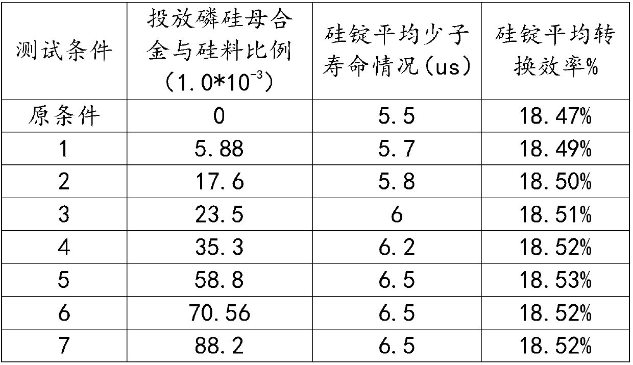
[0029] S1: Preparation of the polycrystalline furnace: Install the quartz rod on the upper part of the polycrystalline furnace, stretch the quartz rod to the bottom and mark it as zero, then raise the quartz rod, and install phosphorus weighing 20.34g in the argon gas pipeline Silicon master alloy. The phosphorus-silicon master alloy is obtained by diluting 100% phosphorus powder with 100% silicon by crystal pulling, and the size of the phosphorus-silicon master alloy is 1-15 mm. The resistivity of the phosphorus-silicon master alloy is greater than 0.0011Ω·cm. It is to convert the set target resistivity value into the gettering crystal concentration value according to the graphical method, table method or calculation method, so as to determine the input amount of the getterin...
Embodiment 2
[0038] A method for increasing the minority carrier lifetime at the top of a silicon ingot by gettering, using the polycrystalline semi-melting process to cast the ingot, includes the following steps:
[0039] S1: Preparation of the polycrystalline furnace: Install the quartz rod on the upper part of the polycrystalline furnace, stretch the quartz rod to the bottom and mark it as zero, then lift the quartz rod, and install phosphorus weighing 50.12g in the argon gas pipeline Silicon master alloy. The phosphorus-silicon master alloy is obtained by diluting 100% phosphorus powder with 100% silicon by crystal pulling, and the size of the phosphorus-silicon master alloy is 1-15 mm. The resistivity of the phosphorus-silicon master alloy is greater than 0.0011Ω·cm. It is to convert the set target resistivity value into the gettering crystal concentration value according to the graphical method, table method or calculation method, so as to determine the input amount of the gettering...
Embodiment 3
[0048] A method for increasing the minority carrier lifetime at the top of a silicon ingot by gettering, using the polycrystalline semi-melting process to cast the ingot, includes the following steps:
[0049] S1: Preparation of the polycrystalline furnace: Install the quartz rod on the upper part of the polycrystalline furnace, stretch the quartz rod to the bottom and mark it as zero, then raise the quartz rod, and install phosphorus with a weight of 12.04g in the argon gas pipeline Silicon master alloy. The phosphorus-silicon master alloy is obtained by diluting 100% phosphorus powder with 100% silicon by crystal pulling, and the size of the phosphorus-silicon master alloy is 1-15 mm. The resistivity of the phosphorus-silicon master alloy is greater than 0.0011Ω·cm. It is to convert the set target resistivity value into the gettering crystal concentration value according to the graphical method, table method or calculation method, so as to determine the input amount of the ...
PUM
| Property | Measurement | Unit |
|---|---|---|
| Size | aaaaa | aaaaa |
| Resistivity | aaaaa | aaaaa |
Abstract
Description
Claims
Application Information
 - R&D Engineer
- R&D Manager
- IP Professional
- Industry Leading Data Capabilities
- Powerful AI technology
- Patent DNA Extraction
Browse by: Latest US Patents, China's latest patents, Technical Efficacy Thesaurus, Application Domain, Technology Topic, Popular Technical Reports.
© 2024 PatSnap. All rights reserved.Legal|Privacy policy|Modern Slavery Act Transparency Statement|Sitemap|About US| Contact US: help@patsnap.com