Eureka AIR delivers breakthrough ideas for toughest innovation challenges, trusted by R&D personnel around the world.

IGBT layout capable of carrying out terminal transverse puncture tests

A technology of lateral withstand voltage and layout, applied in electrical components, electrical solid devices, circuits, etc., can solve the problems of insufficient withstand voltage, insufficient withstand voltage in the terminal area, and insufficient withstand voltage in the cell area, and achieve a good guiding role. Effect

Inactive Publication Date: 2018-01-12
GLOBAL ENERGY INTERCONNECTION RES INST CO LTD +3
View PDF7 Cites 1 Cited by
  • Summary
  • Abstract
  • Description
  • Claims
  • Application Information

AI Technical Summary

Problems solved by technology

The forward blocking voltage test of the IGBT can be tested at two stages before thinning and after tape-out, in order to confirm whether the withstand voltage problem is caused by insufficient thickness of the base region, or is related to improper setting of the field stop layer on the back surface, but it is currently impossible Specifically confirm whether it is caused by the insufficient withstand voltage of the cell area or the insufficient withstand voltage of the terminal area, which is not conducive to the solution of the insufficient withstand voltage problem

Method used


Image

  • IGBT layout capable of carrying out terminal transverse puncture tests
  • IGBT layout capable of carrying out terminal transverse puncture tests

Examples


Embodiment Construction

[0014] The present invention will be further described below with reference to the specific drawings and embodiments.

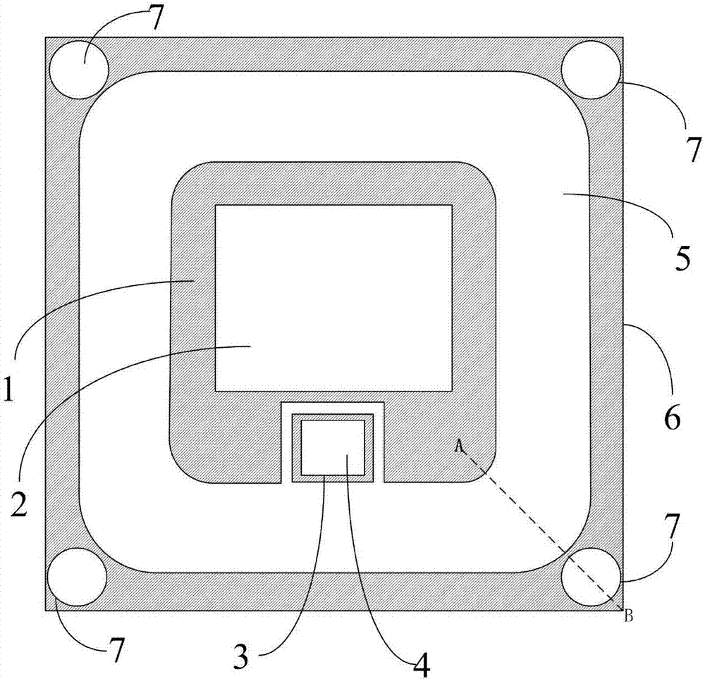
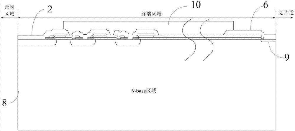
[0015] like figure 1 Shown: In order to effectively carry out the lateral withstand voltage test of the terminal and help to determine the condition of insufficient withstand voltage of the IGBT, the present invention includes a semiconductor substrate, a cell area is arranged in the central area of ​​the semiconductor substrate, and a terminal located in the outer circle of the cell area is provided. Area 5, a source metal 1 and a source pressure pad 2 electrically connected to the source metal 1 are arranged above the cell area; it also includes an auxiliary test pressure pad 7 used to lead out the base area of ​​the terminal area 5, so The auxiliary test pads 7 are located above the terminal area 5 .

[0016] Specifically, the cell region is used to form the functional region of the IGBT device, the terminal region 5 is used to protect the cell region and...


PUM


Abstract

The invention relates to an IGBT layout, in particular to an IGBT layout capable of carrying out terminal transverse puncture tests, and belongs to the technical field of IGBT devices. According to the technical scheme, the IGBT layout capable of carrying out the terminal transverse puncture tests includes a semiconductor substrate, a cellular area and a terminal area which is located at the outerring of the cellular area are arranged at the center area of the semiconductor substrate, and source electrode metal and a source electrode press welding spot which is electrically connected to the source electrode metal are arranged above the cellular area; the IGBT layout further includes an auxiliary press welding spot for leading out a terminal area base region, and the auxiliary press welding spot is located above a terminal area. The IGBT layout is compact in structure, can effectively carry out the terminal transverse puncture tests and is conducive to determining the condition that anIGBT is insufficient in pressure resistance.

Description

technical field [0001] The invention relates to an IGBT layout, in particular to an IGBT layout capable of performing a terminal lateral withstand voltage test, and belongs to the technical field of IGBT devices. Background technique [0002] Insulated gate bipolar transistors (IGBTs) combine the advantages of high current density, low on-resistance and high input impedance of MOS devices of bipolar devices (BJTs), and are used in various power conversion, motor drive and power electronic devices. has been widely used. The forward blocking voltage of IGBT is one of its important static parameters. The IGBT manufacturing process generally includes the front-side MOS manufacturing process, and the backside thinning process of the silicon wafer after the front-side MOS is completed (thinned to the required thickness), and the backside collector fabrication (the backside injection activation, backside metallization process). The forward blocking voltage of the IGBT is not onl...

Claims


Application Information

Patent Timeline
Patent Type & Authority Applications(China)
IPC IPC(8): H01L23/544H01L29/739
Inventor 董少华杨晓鸾许生根姜梅金锐崔磊
Owner GLOBAL ENERGY INTERCONNECTION RES INST CO LTD
Why Eureka
Eureka Blog
Learn More