Laser annealing apparatus and method

A laser annealing and laser technology, which is applied in the manufacture of electrical components, circuits, semiconductors/solid-state devices, etc., can solve the problems of low degree of control freedom, inability to take measures to eliminate pattern effects, poor process adaptability, etc.

Active Publication Date: 2019-10-25
SHANGHAI MICRO ELECTRONICS EQUIP (GRP) CO LTD
View PDF6 Cites 0 Cited by
  • Summary
  • Abstract
  • Description
  • Claims
  • Application Information

AI Technical Summary

Problems solved by technology

[0013] 1. The pattern effect cannot be completely eliminated: on the one hand, when the polarized light in the orthogonal direction interacts with the surface of the silicon wafer to be processed, it will still be partially absorbed; on the other hand, the theoretical Brewster angle can only be infinite Approximate, and for a spot with a certain spatial distribution, it must have a certain distribution near the Brewster angle, so the incident light in the above-mentioned specific polarization direction also has a pattern effect;
[0014] 2. Poor process adaptability and low degree of control freedom: For complex and changeable silicon wafer surface patterns, corresponding measures to eliminate pattern effects cannot be taken

Method used


Image

  • Laser annealing apparatus and method
  • Laser annealing apparatus and method
  • Laser annealing apparatus and method

Examples


Embodiment Construction

[0063] The following will combine Figure 1 to Figure 6 The annealing device for improving annealing uniformity based on reflectivity distribution provided by the present invention is described in detail, which is an optional embodiment of the present invention. It can be considered that those skilled in the art can, within the scope of not changing the spirit and content of the present invention, Revise and polish it.

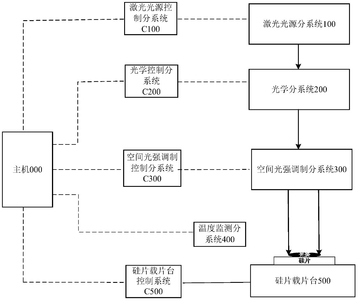
[0064] The present invention provides an annealing device for improving annealing uniformity based on reflectivity distribution, including a host 000, a laser light source subsystem 100, an optical subsystem 200, a spatial light intensity modulation subsystem 300, and a temperature monitoring subsystem 400, wherein:

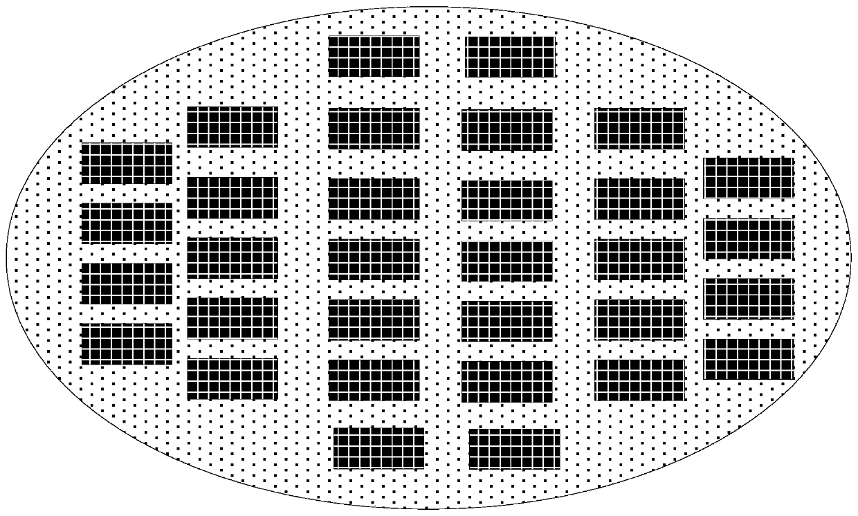
[0065] The temperature monitoring subsystem 400 monitors the temperature at the laser irradiation position on the surface of the silicon wafer and feeds it back to the host; in other words, it monitors the temperature of the laser irradiation are...


PUM


Abstract

The present invention provides a laser annealing apparatus and a laser annealing method. The laser annealing apparatus comprises: a laser light source subsystem controlled by a host machine to generate and output laser; a temperature monitoring subsystem for monitoring the temperatures of silicon wafer surface positions irradiated by the laser, and feeding back to the host machine; an optical subsystem controlled by the host machine to shape and transmit the laser output by the laser light source subsystem to obtain light spots with uniform light intensity distribution; and a space light intensity modulation subsystem controlled by the host machine to modulate the laser emitted by the optical subsystem so as to make the light intensity distribution of the light spot incident at the siliconwafer surface position be corresponding to the reflectivity of the silicon wafer surface, such that the energies absorbed by each light spot position on the silicon wafer surface are consistent, andthe energies can be determined according to the monitored temperatures, wherein the host machine controls the laser light source subsystem, the optical subsystem and the space light intensity modulation subsystem according to the feedback of the temperature monitoring subsystem.

Description

technical field [0001] The invention relates to the field of silicon wafer processing, in particular to an annealing device and method after silicon wafer photolithography. Background technique [0002] Driven by Moore's Law, chip manufacturing has experienced rapid growth over the past few decades. This continued rapid development stems from the continued shrinking of chip size. Correspondingly, this smaller size brings more and more difficulties and challenges to the processing and manufacturing process of the chip. The traditional silicon wafer rapid thermal annealing method has been difficult to meet the requirements of 45nm and higher nodes. Alternatives to new annealing techniques are being intensively researched. [0003] Due to the development of laser application technology in recent years, laser annealing technology has shown a good application prospect. Compared with traditional annealing, laser annealing has a small thermal budget and high activation efficien...

Claims


Application Information

Patent Timeline
Patent Type & Authority Patents(China)
IPC IPC(8): H01L21/268
Inventor 崔国栋马明英朱树存孙刚
Owner SHANGHAI MICRO ELECTRONICS EQUIP (GRP) CO LTD
Why Eureka
Try Eureka