A flexible touch motherboard and its preparation method, flexible touch substrate, touch panel

A flexible touch and motherboard technology, applied in semiconductor/solid-state device manufacturing, instruments, semiconductor devices, etc., to achieve low square resistance, avoid bubbling defects, and improve product yield

Active Publication Date: 2020-07-24
BOE TECH GRP CO LTD +1
View PDF8 Cites 0 Cited by
  • Summary
  • Abstract
  • Description
  • Claims
  • Application Information

AI Technical Summary

Problems solved by technology

[0006] In view of this, in order to solve the problems of the prior art, the embodiments of the present invention provide a flexible touch control motherboard and a preparation method, a flexible touch substrate, and a touch panel, which can reduce the square resistance of electrodes and improve the electrode film. The problem of uneven stress in the layer can avoid the problem of poor bubbling in the subsequent protective layer and improve the product yield

Method used


Image

  • A flexible touch motherboard and its preparation method, flexible touch substrate, touch panel
  • A flexible touch motherboard and its preparation method, flexible touch substrate, touch panel
  • A flexible touch motherboard and its preparation method, flexible touch substrate, touch panel

Examples


Embodiment 1

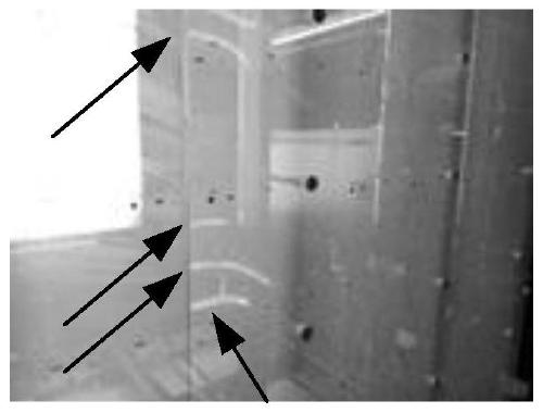
[0037] The embodiment of the present invention provides a method for preparing a flexible touch motherboard, such as figure 2 As shown, the preparation method includes,

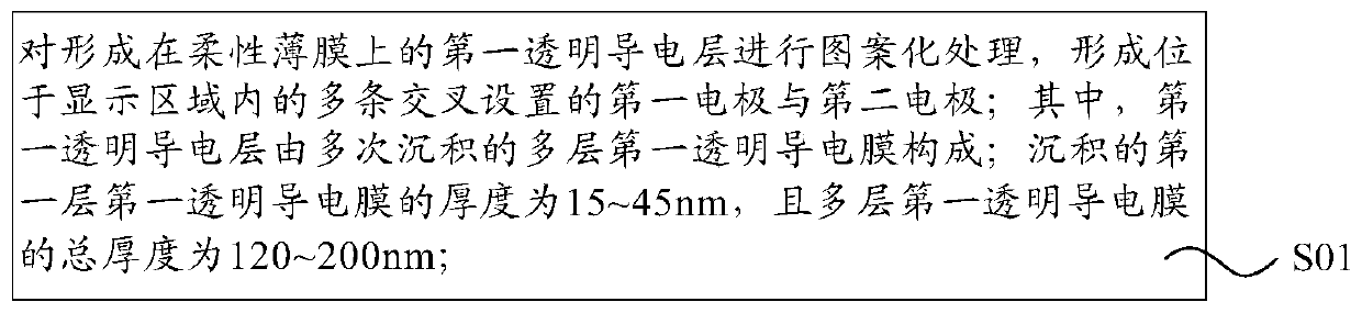
[0038] Step S01, patterning the first transparent conductive layer formed on the flexible film to form a plurality of intersecting first electrodes and second electrodes located in the display area; wherein, the first transparent conductive layer is deposited by multiple times The multi-layer first transparent conductive film is formed; the thickness of the deposited first layer of the first transparent conductive film is 15-45nm, and the total thickness of the multi-layer first transparent conductive film is 120-200nm.

[0039] It should be noted that, first, the above-mentioned flexible touch motherboard provided by the embodiment of the present invention includes multiple display areas, which can be divided into multiple small pieces, that is, a single flexible touch substrate, each flexible Each touch su...

Embodiment 2

[0088] Furthermore, the embodiment of the present invention also provides a flexible touch control board, which is prepared by the above preparation method. It can obtain a relatively flat surface while having a low electrode channel impedance, and is the first in the industry to realize the Roll to Sheet low square resistance process.

Embodiment 3

[0090] Furthermore, the embodiment of the present invention also provides a flexible touch substrate, which is any one of the multiple sub-substrates cut from the above-mentioned flexible touch motherboard.


PUM

PropertyMeasurementUnit
thicknessaaaaaaaaaa
thicknessaaaaaaaaaa
thicknessaaaaaaaaaa

Abstract

Embodiments of the present invention provide a flexible touch motherboard and a preparation method, a flexible touch substrate, and a touch panel, which relate to the field of display technology, can reduce square resistance and improve film layer stress, avoid bubbling defects, and improve product quality. Rate. The preparation method includes patterning the first transparent conductive layer formed on the flexible film to form the first and second electrodes; the first transparent conductive layer is composed of multi-layered first transparent conductive films deposited multiple times; the deposited The thickness of the first layer of the first transparent conductive film is 15-45nm, and the total thickness of the multi-layer first transparent conductive film is 120-200nm.

Description

technical field [0001] The invention relates to the field of display technology, in particular to a flexible touch control motherboard and a preparation method, a flexible touch control substrate, and a touch panel. Background technique [0002] With the gradual development of narrow frame and no frame of flexible touch display products, the space for flexible touch electrodes (i.e. Sensor) wiring at the edge of the frame will be further reduced. Low channel impedance to reduce surface resistance (or square resistance). The symbol of the square resistance is Rs, and the expression is Rs=ρ / t; where, ρ is the resistivity of the electrode material, and t is the thickness of the electrode. [0003] Sensor is usually made of ITO (Indium Tin Oxide, Indium Tin Oxide) transparent conductive material. At present, the square resistance of ITO commonly used in the industry is 100Ω / □ (the symbol "□" indicates a square). In order to reduce the in-plane resistance, the ITO square resista...

Claims


Application Information

Patent Timeline
Patent Type & Authority Patents(China)
IPC IPC(8): H01L27/32H01L21/56
CPCH01L21/56H10K59/40H10K59/12H10K59/131G06F2203/04111G06F2203/04102G06F2203/04103G06F3/0446G06F3/0443G09G3/20G06F3/0412B32B2307/202B32B2307/412
Inventor 曾亭张明李红军陈启程张由婷殷刘岳
Owner BOE TECH GRP CO LTD
Why Eureka
Try Eureka