Biaxial-crystal electro-optical Q switch and fabrication method thereof
An electro-optical and switching technology, applied in circuits, lasers, electrical components, etc., can solve problems such as the influence of temperature stability of Q-switching switches, and achieve the effect of low insertion loss, simple operation, and solving influences.
- Summary
- Abstract
- Description
- Claims
- Application Information
AI Technical Summary
Problems solved by technology
Method used
Image
Examples
Embodiment approach
[0061] The second embodiment of the present invention provides a second specific implementation of a biaxial crystal electro-optical Q-switch, see Figure 4 , the electro-optical Q-switch specifically includes the following contents:
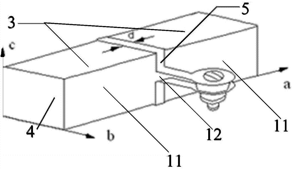
[0062] The electro-optical Q-switch includes: two electro-optical crystal elements 21 with the same shape, and a phase compensation wave plate 22 arranged between the two electro-optical crystal elements 21 along the light passing direction, and the c of the electro-optical crystal element 21 Electrode layers 3 are plated on both sides.
[0063] The electro-optical crystal element 21 and the phase compensation wave plate 22 are both rectangular biaxial electro-optical crystals of the same type.
[0064] The two electro-optic crystal elements 21 and the phase compensating wave plate 22 are bonded together by thermal bonding technology.
[0065] Compared with the first embodiment, the electro-optical crystal element 21 and the phase compensation...
specific Embodiment approach 2
[0078] Embodiment 4 of the present invention provides a specific embodiment 2 of a method for manufacturing a biaxial crystal electro-optical Q-switch corresponding to embodiment 1, see Figure 7 , the preparation method of the electro-optical Q-switch specifically includes the following contents:
[0079] Step 201 : cutting the original biaxial crystal electro-optical crystal according to the direction of electro-optical application to obtain a rectangular biaxial electro-optical crystal.
[0080] Step 202: Perform precise optical polishing on the light-transmitting surface 4 of the electro-optic crystal element 11 obtained by cutting.
[0081] Step 203 : A detachable metal collar 5 is arranged on the outer wall of the phase compensation wave plate 12 , and the inner wall of the metal collar 5 is closed and adhered to the outer wall of the phase compensation wave plate 12 .
[0082] Step 204 : Coating the electrode layer 3 on the two c-direction surfaces extending along the ...
PUM
 Abstract
Description
Claims
Application Information
 - R&D Engineer
- R&D Manager
- IP Professional
- Industry Leading Data Capabilities
- Powerful AI technology
- Patent DNA Extraction
Browse by: Latest US Patents, China's latest patents, Technical Efficacy Thesaurus, Application Domain, Technology Topic, Popular Technical Reports.
© 2024 PatSnap. All rights reserved.Legal|Privacy policy|Modern Slavery Act Transparency Statement|Sitemap|About US| Contact US: help@patsnap.com


