
Baking device for curing SMD LED glue and method thereof

A baking device and glue curing technology, applied in the field of LED baking, can solve the problems of fluorescent powder precipitation and inconsistent distribution, high labor intensity of technicians, inflexible and inconvenient use, etc., to improve energy utilization and luminous flux , Good effect of color consistency

Pending Publication Date: 2017-12-08
SUZHOU HANRAYSUN OPTOELECTRONICS
View PDF4 Cites 4 Cited by
  • Summary
  • Abstract
  • Description
  • Claims
  • Application Information

AI Technical Summary

Problems solved by technology

[0002] At present, the oven body of LED baking equipment is usually fixed on the workbench, which is not flexible and inconvenient to use. Putting the LED in a small space, due to the separation of multiple partitions, it is easy to cause the uneven distribution of the hot air source for baking, so that the quality of the product is not stable enough when the LED is packaged, and there is a large difference. The baked LEDs need to be put into the oven one by one. The labor intensity of the technicians is high, which reduces the work efficiency. A process of structural cured products. In this process, due to the difference in the particle size of the phosphor powder added, there are inconsistencies in the precipitation and distribution of the phosphor powder, which will affect the consistency of the color, and the brightness will be scattered.

Method used


Image

  • Baking device for curing SMD LED glue and method thereof
  • Baking device for curing SMD LED glue and method thereof
  • Baking device for curing SMD LED glue and method thereof

Examples


Embodiment Construction

[0023] Below in conjunction with specific embodiment, content of the present invention is described in further detail:

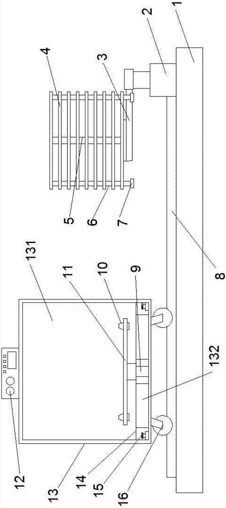
[0024] refer to figure 1 , an LED baking device, including a workbench 1, an oven body 13 and a feeding assembly, the workbench 1 is provided with a guide rail 8 and a feeding assembly, the four corners below the oven body 13 are provided with pulleys 16, the The pulley 16 cooperates with the guide rail 8, and the inside of the oven is provided with a motor 9, the output shaft of the motor 9 is fixedly connected with the center hole of the bottom 11 of the square fixed plate, and four corners of the square fixed plate 11 are symmetrically arranged with four A claw 10, a baking frame is provided on the feeding assembly, and a block 7 is provided at the bottom of the baking frame, and the block 7 is used in conjunction with the claw 10.

[0025] The baking frame includes a central column 5, at least two layers of baking trays 4 and pillars 6, the baking tray ...


PUM


Abstract

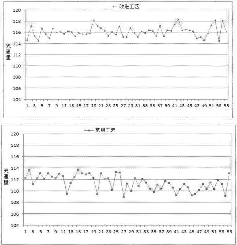
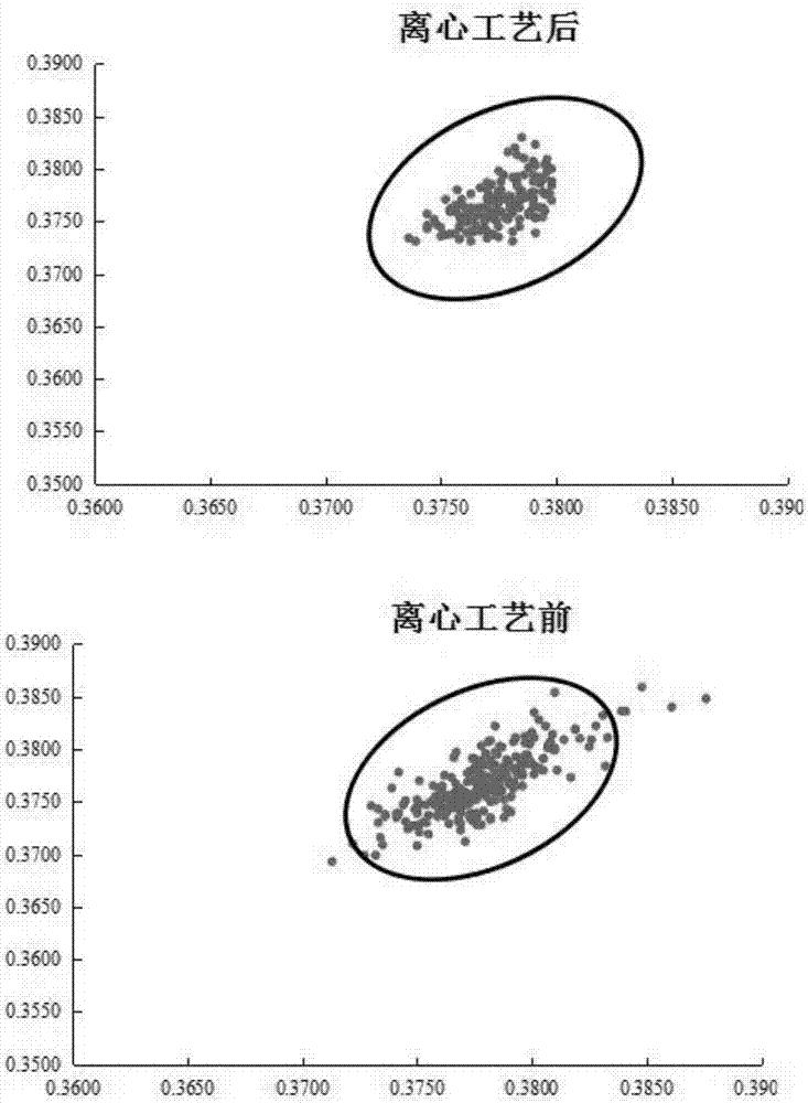
The invention relates to the technical field of baking of LED and particularly relates to a baking device for curing SMD LED glue and a method thereof. The baking device is simple in structure, high in using efficiency and flexible to operate, and is capable of baking a large number of LED lamps in one time; a removable baking frame is arranged on a feeding component; LED lamps to be baked are directly mounted on the baking frame outside a baking oven; clamping jaws of a square fixed disc are matched with clamping blocks of the braking frame in use, so that the operating efficiency is greatly improved; the baking frame carrying LEDs is directly carried into the baking oven or taken out of the baking oven by a machine, and then a next baking frame is put in the baking oven, so that the energy utilization rate and the baking efficiency are improved; the motor drives the baking frame on the square fixed disc to slowly rotate; when the baking device is used in the later period of baking, the stability of the quality of LEDs can be improved; through the method for baking SMD LED chips by using the baking device for curing SMD LED glue, the fluorescent powder sediment is more uniformly distributed; the color consistency is higher; the scattered property of luminance is slow; compared with the luminous flux of the conventional process, the luminous flux of the method is increased by about 3%.

Description

technical field [0001] The invention relates to the technical field of LED baking, in particular to a baking device and method for curing SMD LED glue. Background technique [0002] At present, the oven body of LED baking equipment is usually fixed on the workbench, which is not flexible and inconvenient to use. Putting the LED in a small space, due to the separation of multiple partitions, it is easy to cause the uneven distribution of the hot air source for baking, so that the quality of the product is not stable enough when the LED is packaged, and there is a large difference. The baked LEDs need to be put into the oven one by one. The labor intensity of the technicians is high, which reduces the work efficiency. A process of structural cured products. In this process, due to the difference in the particle size of the phosphor powder added, there are inconsistencies in the precipitation and distribution of the phosphor powder, which will affect the consistency of the col...

Claims


Application Information

Patent Timeline
Patent Type & Authority Applications(China)
IPC IPC(8): B05D3/02H01L33/48
CPCH01L33/48B05D3/0254H01L2933/0033
Inventor 占贤武黄德凯
Owner SUZHOU HANRAYSUN OPTOELECTRONICS
Learn More