Adhesive packaging method of light emitting diode chip

A light-emitting diode and chip technology, which is applied in the field of sealing glue suitable for forming fluorescent layers and/or lenses on light-emitting diode chips, can solve the problems that the main part of the package cannot be omitted in the finished product, the cost is high, and the mold making is complicated, so as to avoid Mold making complex and costly effects

Inactive Publication Date: 2017-12-05
孔东灿
View PDF4 Cites 0 Cited by
  • Summary
  • Abstract
  • Description
  • Claims
  • Application Information

AI Technical Summary

Problems solved by technology

Most of the traditional manufacturing process is to form the lens after the LED chip is connected on the substrate or lead frame, and finally cut into a single package. Therefore, the finished product also has the disadvantage that the main part of the package cannot be omitted. In addition, the lens is generally It is formed by injecting transparent glue into the mold cavity between the upper mold and the lower mold to cover the LED chip, and then curing it. However, the mold cavity and injection port are formed separately in the upper and lower molds, which will lead to complex mold making and high cost. Disadvantages such as expensive, and the side of the lens may form a cut vertical wall due to the cutting step

Method used


Image

  • Adhesive packaging method of light emitting diode chip
  • Adhesive packaging method of light emitting diode chip
  • Adhesive packaging method of light emitting diode chip

Examples


Embodiment Construction

[0046] Various preferred embodiments of the present invention will be described below with reference to the accompanying drawings. The following description with reference to the accompanying drawings is provided to assist understanding of example embodiments of the invention as defined by the claims and their equivalents. It includes various specific details to aid in understanding but they are to be regarded as exemplary only. Accordingly, those of ordinary skill in the art will recognize that various changes and modifications of the embodiments described herein can be made without departing from the scope and spirit of the invention. Also, detailed descriptions of functions and constructions well-known in the art will be omitted to make the description clearer and more concise.

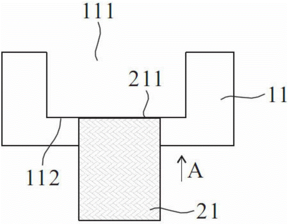
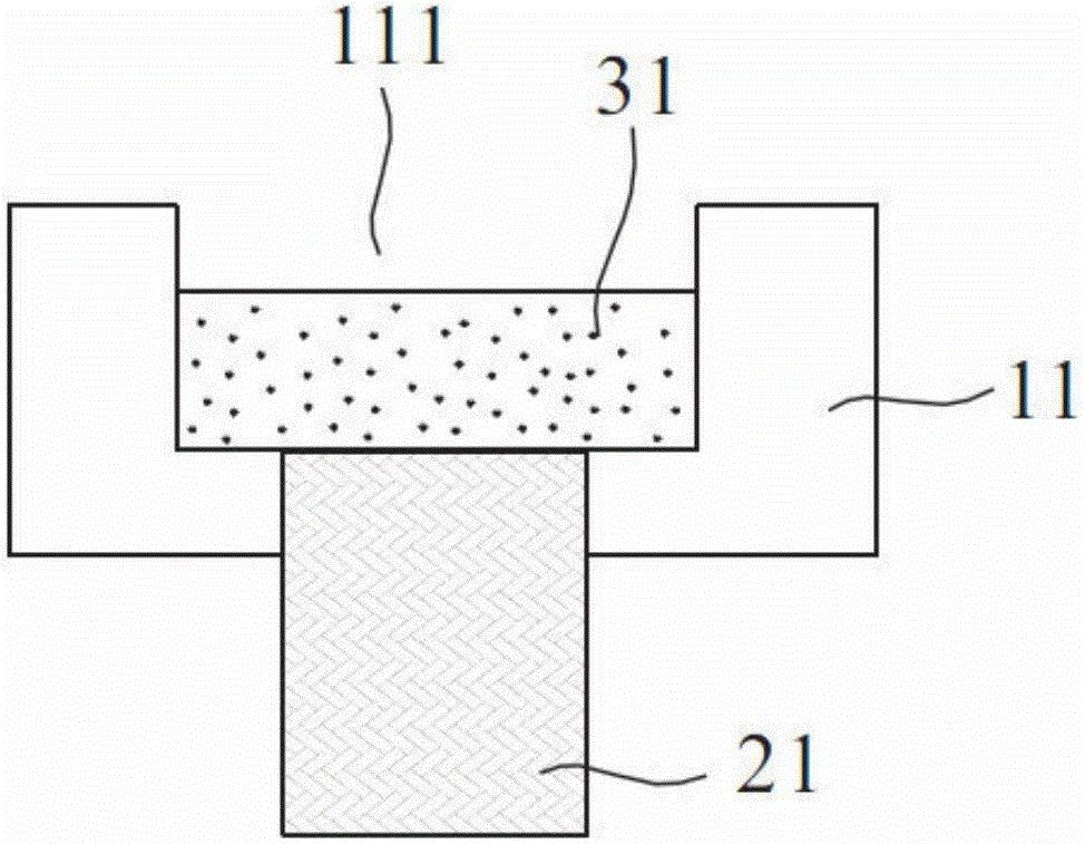
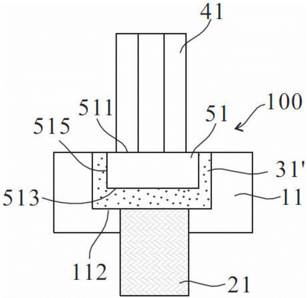
[0047] See Figure 1-7 , which is a schematic cross-sectional view of the production process of the first sealing product according to the first embodiment of the present invention.

[0048] Fir...


PUM


Abstract

A method for encapsulating LED chips, comprising: providing a first forming mold with a first mold cavity; filling a first encapsulant into the first mold cavity; placing the LED chip into the first mold cavity, Encapsulating the LED chip with the first encapsulation material, wherein the active surface of the LED chip is facing outward and not covered by the first encapsulation material; and curing the first encapsulation material to form a first encapsulation finished product. Accordingly, the present invention can directly coat the light-emitting diode chip with a packaging material such as fluorescent glue or transparent glue, so as to save the main part of the package such as the lead frame/substrate, which is beneficial to thinner design.

Description

technical field [0001] The invention relates to a glue sealing method for a light emitting diode chip, in particular to a glue sealing method suitable for forming a fluorescent layer and / or a lens on the light emitting diode chip. Background technique [0002] Compared with traditional light sources, light-emitting diodes (LEDs) have the advantages of power saving, small size, and no heat radiation. Therefore, in recent years, light-emitting diodes have gradually replaced traditional light sources. However, most light-emitting diodes are red, yellow, green, and blue light sources. Therefore, in order to meet the needs of various light colors, LED chips with different colors or coated with a fluorescent layer on the outer layer of the LED are generally used to make use of mixed light. to produce the desired shade. [0003] In the prior art LED production process, the LED wafer can be cut into single LED chips first, then the LED chips are fixed on the substrate or lead frame...

Claims


Application Information

Patent Timeline
Patent Type & Authority Applications(China)
IPC IPC(8): H01L33/56H01L33/50H01L33/00
CPCH01L33/005H01L33/502H01L33/56
Inventor 孔东灿
Owner 孔东灿
Why Eureka
Try Eureka