Preparation method of niobium-doped stannic oxide monocrystal film with high migration rate

A single crystal thin film and tin oxide technology, which is applied in the field of preparation of high mobility niobium doped tin oxide single crystal thin film, can solve the problems that are difficult to meet the application standards of devices, high mobility and low defect density, and affect the electrical properties of materials, etc. , to achieve the effect of excellent photoelectric performance, excellent electrical and optical performance, and easy industrial production

Inactive Publication Date: 2017-12-01
SHANDONG UNIV
View PDF7 Cites 10 Cited by
  • Summary
  • Abstract
  • Description
  • Claims
  • Application Information

AI Technical Summary

Problems solved by technology

SnO prepared under existing technical conditions 2 It is difficult for thin-film materials to meet the standards for device applications, mainly because it is difficult to obtain single-crystal SnO with high mobility and low defect density by traditional preparation techniques. 2 Doped thin film materials seriously affect the electrical properties of the material

Method used


Image

  • Preparation method of niobium-doped stannic oxide monocrystal film with high migration rate
  • Preparation method of niobium-doped stannic oxide monocrystal film with high migration rate
  • Preparation method of niobium-doped stannic oxide monocrystal film with high migration rate

Examples


Embodiment 1

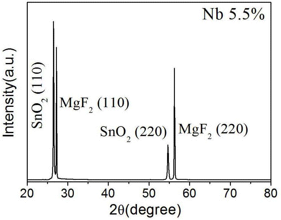
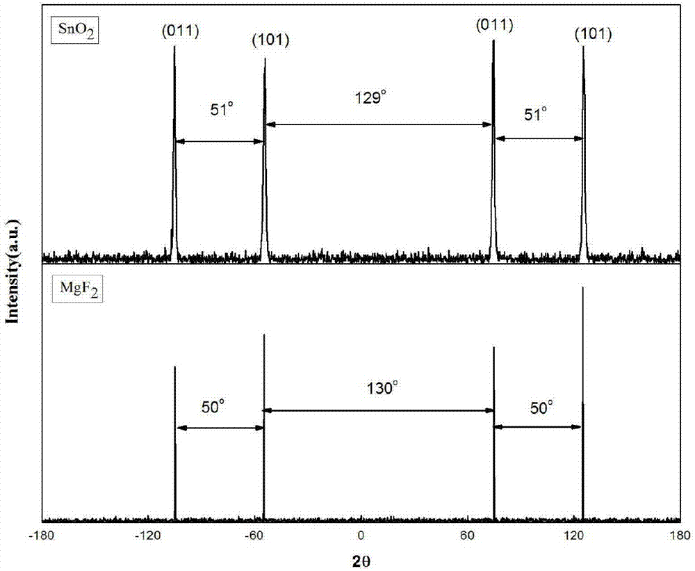
[0061] Example 1: Nb doping ratio is 5.5%

[0062] Nb-doped tin oxide thin film materials were prepared by MOCVD technology. The polished magnesium fluoride (110) surface was used as the substrate, and Sn(C 2 h 5 ) 4 As an organometallic tin source, Nb(C 2 h 5 O) 5 As an organometallic niobium source, the steps are as follows:

[0063] (1) First pump the reaction chamber of the MOCVD equipment to a high vacuum state of 5×10 -4 Pa, heat the substrate to 660°C;

[0064] (2) Open the valve of the nitrogen cylinder and feed nitrogen into the reaction chamber (background N 2 )500sccm, 30 minutes, make the reaction chamber pressure

[0065] The strong is 30Torr;

[0066] (3) Open the valve of the oxygen cylinder, adjust the flow rate of oxygen to 50 sccm, and keep it for 10 minutes;

[0067] (4) Open the valve of the organometallic Sn source bottle and adjust the carrier gas N 2 Flow 20sccm, keep for 10 minutes;

[0068] (5) open the organometallic Nb source bottle valve...

Embodiment 2

[0076] Example 2: Preparation of niobium-doped single crystal tin oxide thin film material by MOCVD technology, changing the Nb doping ratio

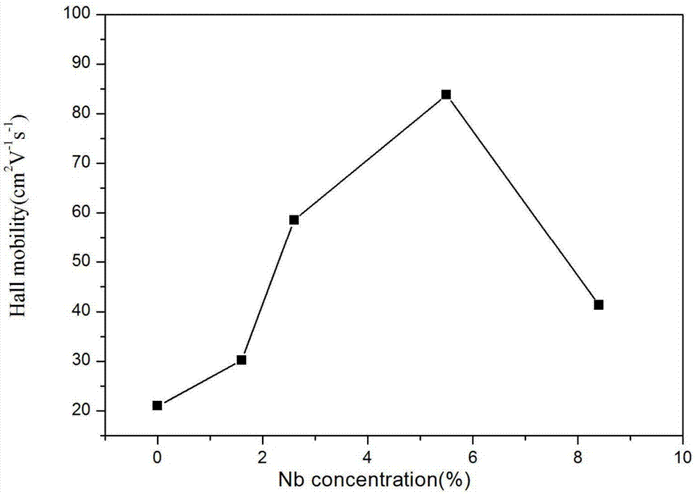
[0077] The preparation steps are as described in Example 1, the difference is that the flow rate of the Nb source is changed, so that the Nb doping ratio is 1.6%, 2.6% and 8.4%, and the prepared films are all single crystal structures, and the carrier migration of the films Rate is 30.2cm 2 V -1 the s -1 、58.5cm 2 V -1 the s -1 and 41.3cm 2 V -1 the s -1 , with the increase of Nb doping ratio, the Hall shift of the film first increases and then decreases, as image 3 shown. The average relative transmittance in the visible light range is 74%, 80% and 68%, respectively, such as Figure 4 shown.


PUM

PropertyMeasurementUnit
thicknessaaaaaaaaaa
optical band gapaaaaaaaaaa
thicknessaaaaaaaaaa

Abstract

The invention relates to a preparation method of niobium-doped stannic oxide monocrystal film with a high migration rate. The method comprises the step of using an MOCVD method to grow the niobium-doped stannic oxide monocrystal film on a magnesium fluoride substrate under the condition of vacuum by using tetraethyltin and niobium ethoxide as metal organic sources, using oxygen as an oxidizing gas, and using nitrogen as a carrier gas. The stannic oxide film is an epitaxial material with a monocrystal structure, no twin crystal and domain structure exist in the film, the carrier migration rate of the niobium-doped stannic oxide film is up to 83.8cm<2>V<-1>s<-1>, and average transmittance of a visible light area reaches 83%. The method can be used for preparing transparent semiconductor devices or ultraviolet electronic devices.

Description

technical field [0001] The invention relates to a preparation method of a high-mobility niobium-doped tin oxide single crystal thin film, belonging to the technical field of semiconductor optoelectronic materials. Background technique [0002] Tin oxide (SnO 2 ) is a wide bandgap semiconductor material with a direct bandgap. Compared with gallium nitride (GaN, Eg ~ 3.4eV) and zinc oxide (ZnO, Eg ~ 3.37eV, exciton binding energy ~ 60meV), tin oxide materials not only have a wider band gap and higher excitonic Binding energy (~3.7eV and ~130meV respectively at room temperature), and has the advantages of low preparation temperature and stable physical and chemical properties. So far, the research on tin oxide has mainly focused on the aspects of transparent conductivity, gas-sensing properties and nanomaterial properties. At present, tin oxide thin-film materials are mainly used in transparent electrodes of thin-film solar cells and light-emitting devices, and gas sensors. ...

Claims


Application Information

Patent Timeline
Patent Type & Authority Applications(China)
IPC IPC(8): C30B29/16C30B25/18H01L21/365H01L31/18H01L31/0224H01L33/42
CPCC30B25/18C30B29/16H01L21/0237H01L21/02565H01L21/0257H01L21/02598H01L21/0262H01L31/022425H01L31/022466H01L31/1884H01L33/42H01L2933/0016Y02P70/50
Inventor 栾彩娜马瑾何林安
Owner SHANDONG UNIV
Why Eureka
Try Eureka