Metallization coating method for through hole of film circuit

A thin-film circuit and metallization technology, applied in the field of thin-film circuit through-hole metallization coating, can solve the problems of diffraction and sputtering film layers, etc., and achieve the effect of simple operation, solving peeling off, and easy and easy operation.

Active Publication Date: 2017-12-01
THE 41ST INST OF CHINA ELECTRONICS TECH GRP
View PDF4 Cites 7 Cited by
  • Summary
  • Abstract
  • Description
  • Claims
  • Application Information

AI Technical Summary

Problems solved by technology

[0006] Aiming at the problem that the poor sputtering film layer around the through hole of the thin film circuit substrate is easy to fall off, resulting in an unstable film layer, the present invention provides a coating method for the metallization of the through hole of the thin film circuit, which solves the problems caused by sputtering coating equipment and substrates. Hardware problems lead to diffraction phenomenon around the hole in actual operation, and the difficulty of sputtering film layer is not strong

Method used


Image

  • Metallization coating method for through hole of film circuit
  • Metallization coating method for through hole of film circuit

Examples


Embodiment Construction

[0030] The specific embodiment of the present invention will be further described below in conjunction with accompanying drawing and specific embodiment:

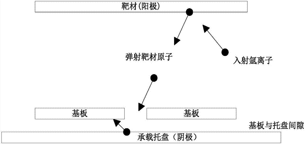
[0031] combine figure 1 and figure 2 , a thin film circuit through-hole metallization coating method, comprising the following steps:

[0032] Step 1: Provide a thin film circuit substrate of the required type and size, and use a laser drilling machine to perform through-hole processing on the thin film circuit substrate.

[0033] The thin film circuit substrate is made of aluminum oxide substrate with a purity of more than 99.6% or an aluminum nitride substrate or a quartz substrate with a purity of 98%, and the thickness of the substrate is 0.1mm to 0.65mm. For example, the selected hard dielectric substrate material is alumina ceramics with a purity of 99.6%, and a thickness of 0.254mm. Use a laser drilling machine, set the spiral interval to 0.01mm, automatically position through the equipment, scan 200 times with an...


PUM

PropertyMeasurementUnit
thicknessaaaaaaaaaa

Abstract

The invention provides a metallization coating method for a through hole of a film circuit. A magnetron sputtering vacuum coating technology is adopted for achieving metallization coating of the through hole of the ceramic circuit. The coating technology has the biggest beneficial effect that deposited materials are not limited and can be used for achieving coating as long as the deposited materials can be made in to target materials. In addition, the coating technology has the beneficial effects that film forming equipment is simple, repeatability is good, the film layer is firm, and the technology is suitable for metallization deposition of base plates with complex patterns, especially base plates with holes. The method that high-temperature adhesive is attached to the back face and then the front face is subjected to metal coating is adopted, so that the problem that during sputtering, the film layer is poor due to diffraction of target material atoms is solved; and in addition, a substrate on the back face is protected against pollution due to the high-temperature adhesive, and the beneficial effects that operation is simple, cost is low, and the attaching force with the substrate is good are achieved. The problem that the diffraction phenomenon happens to the periphery of the hole during practical operation and the sputtered film layer is not firm due to the problems of sputtering coating equipment and base plate hardware is solved.

Description

technical field [0001] The invention relates to the field of thin film circuits, in particular to a metallization coating method for through holes of thin film circuits. Background technique [0002] Miniaturized and highly integrated thin film integrated circuits are widely used in microwave and millimeter wave test instruments. The continuous improvement of the integration level of thin-film hybrid integrated circuit substrates has led to the through-hole metallization technology of microwave ceramics, artificial sapphire, quartz, aluminum nitride and other hard dielectric substrates gradually becoming a research hotspot. [0003] Due to the relatively stable chemical properties of ceramics, the more mature roughening, sensitization, and activated through-hole metallization processes used in organic circuit boards have no effect on the through-hole metallization of ceramics. Thin-film circuits are usually metallized by magnetron sputtering coating (generally sputtering co...

Claims


Application Information

Patent Timeline
Patent Type & Authority Applications(China)
IPC IPC(8): C23C14/35C23C14/02C23C14/18
CPCC23C14/02C23C14/185C23C14/35
Inventor 孙毅许延峰王进马子腾
Owner THE 41ST INST OF CHINA ELECTRONICS TECH GRP
Why Eureka
Try Eureka