Method for using proton irradiation to prepare ultrafast response GaN photoconductive switch
A technology of photoconductive switching and proton irradiation, applied in circuits, electrical components, semiconductor devices, etc., can solve the problems of low on-state current of devices, decrease in film quality, and decrease in mobility, etc., and achieve broad application prospects and great scientific value. Effect
- Summary
- Abstract
- Description
- Claims
- Application Information
AI Technical Summary
Problems solved by technology
Method used
Image
Examples
Embodiment 1
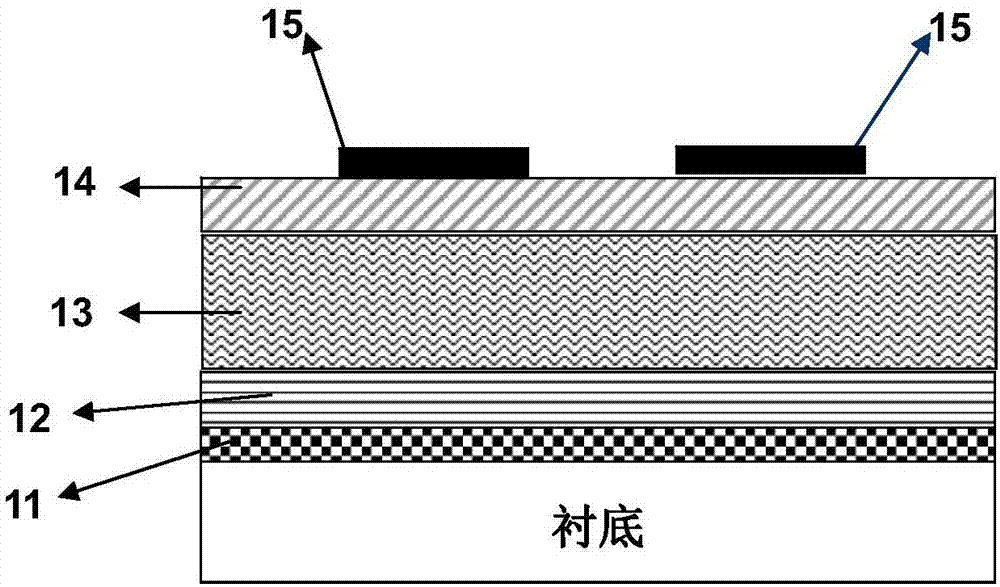
[0043] The GaN photoconductive switch of the present invention comprises, from bottom to top, a sapphire substrate, an AlN nucleation layer 11 , a GaN high temperature buffer layer 12 , an i-GaN layer 13 and an n-GaN layer 14 . The thickness of the AlN nucleation layer 11 is 100nm; the thickness of the GaN high-temperature buffer layer 12 is 1.0μm; the thickness of the i-GaN layer 13 is 100nm, and the electron concentration is 8×10 16 / cm 3 ; The n-GaN layer 14 has a thickness of 100nm and an electron concentration of 1×10 20 / cm 3 . The surface of the n-GaN layer 14 is Ni / Cr / Au parallel ohmic contact metal electrodes 15 with an electrode width of 5mm and an electrode spacing of 0.5mm.
Embodiment 2
[0045] The GaN photoconductive switch of the present invention comprises, from bottom to top, a sapphire substrate, an AlN nucleation layer 11 , a GaN high temperature buffer layer 12 ; an i-GaN layer 13 and an n-GaN layer 14 . Among them, the thickness of the AlN nucleation layer 11 is 80nm; the thickness of the GaN high temperature buffer layer 12 is 1.5μm; the thickness of the i-GaN layer 13 is 400nm, and the electron concentration is 1×10 16 / cm 3 ; The n-GaN layer 14 has a thickness of 150nm and an electron concentration of 6×10 21 / cm 3 . The surface of the n-GaN layer 14 is Ni / Cr / Au parallel ohmic contact metal electrodes 15, the electrode width is 3mm, and the electrode spacing is 3mm.
Embodiment 3
[0047] The GaN photoconductive switch of the present invention comprises, from bottom to top, a sapphire substrate, an AlN nucleation layer 11 , a GaN high temperature buffer layer 12 , an i-GaN layer 13 and an n-GaN layer 14 . Among them, the thickness of the AlN nucleation layer 11 is 180nm; the thickness of the GaN high-temperature buffer layer 12 is 1.2μm; the thickness of the i-GaN layer 13 is 200nm, and the electron concentration is 2×10 17 / cm 3 ; The n-GaN layer 14 has a thickness of 50nm and an electron concentration of 6×10 21 / cm 3 . The surface of the n-GaN layer 14 is Ni / Cr / Au parallel ohmic contact metal electrodes 15 with an electrode width of 0.5mm and an electrode spacing of 5mm.
PUM
 Abstract
Description
Claims
Application Information
 - R&D
- Intellectual Property
- Life Sciences
- Materials
- Tech Scout
- Unparalleled Data Quality
- Higher Quality Content
- 60% Fewer Hallucinations
Browse by: Latest US Patents, China's latest patents, Technical Efficacy Thesaurus, Application Domain, Technology Topic, Popular Technical Reports.
© 2025 PatSnap. All rights reserved.Legal|Privacy policy|Modern Slavery Act Transparency Statement|Sitemap|About US| Contact US: help@patsnap.com


