Preparation method of diode and diode

A diode, N-type technology, used in semiconductor/solid-state device manufacturing, semiconductor devices, electrical components, etc., can solve the problems of zero reverse recovery time, low on-state voltage drop, on-state voltage drop, etc.

Active Publication Date: 2017-11-14
FOUNDER MICROELECTRONICS INT
View PDF3 Cites 2 Cited by
  • Summary
  • Abstract
  • Description
  • Claims
  • Application Information

AI Technical Summary

Problems solved by technology

[0006] In related technologies, Schottky diodes have low on-state voltage drop, large leakage current, and almost zero reverse recovery time
The photodiode has a fast reverse recovery time, but its on-state voltage drop is high

Method used


Image

  • Preparation method of diode and diode
  • Preparation method of diode and diode
  • Preparation method of diode and diode

Examples


Embodiment Construction

[0028] In order to understand the above-mentioned purpose, features and advantages of the present invention more clearly, the present invention will be further described in detail below in conjunction with the accompanying drawings and specific embodiments. It should be noted that, in the case of no conflict, the embodiments of the present application and the features in the embodiments can be combined with each other.

[0029] In the following description, many specific details are set forth in order to fully understand the present invention. However, the present invention can also be implemented in other ways different from those described here. Therefore, the protection scope of the present invention is not limited by the specific details disclosed below. EXAMPLE LIMITATIONS.

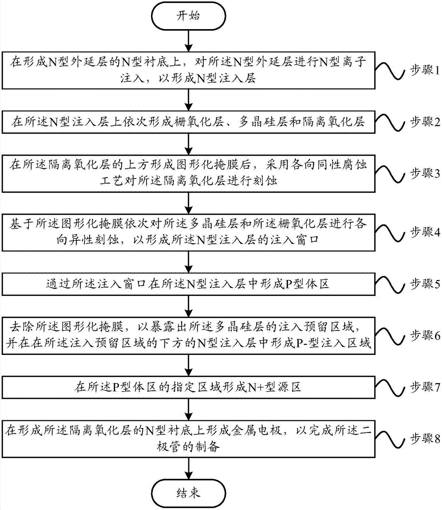
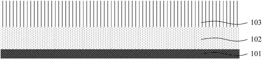
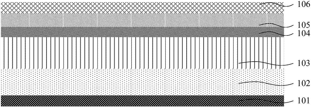
[0030] figure 1 A schematic flow chart showing a method for preparing a diode according to an embodiment of the present invention

[0031] Such as figure 1 As shown, the method for preparing a dio...


PUM


Abstract

The present invention provides a preparation method of a diode and a diode. The preparation method of the diode comprises the following steps that: N type ion implantation is performed on an N type epitaxial layer; a gate oxide layer, a polysilicon layer and an isolation oxide layer are sequentially formed on the N type implant layer; an isotropic etching process is adopted to etch the isolation oxide layer; anisotropic etching is performed on the polysilicon layer and the gate oxide layer based on a patterned mask; P type body regions are formed in the N type implantation layer through injection windows; the patterned mask is removed, so that implantation reserved regions of the polysilicon layer can be exposed, P- type implantation regions are formed in the N type implantation layer below the implantation reserved regions; N+ type source regions are formed in designated regions of the P type body regions; and a metal electrode is formed on the N type substrate of the isolation oxide layer. A diode prepared by using the preparation method of the invention has the advantages of large reverse voltage, short reverse recovery time, small reverse recovery peak current and the like.

Description

technical field [0001] The invention relates to the technical field of semiconductor manufacturing, in particular to a method for preparing a diode and a diode. Background technique [0002] Power diodes are key components of circuit systems, and are widely used in high-frequency inverters, digital products, generators, televisions and other civilian products, as well as satellite receivers, missiles and aircraft and other advanced weapon control systems and instrumentation equipment. Military occasions. There are two important directions for power diode expansion: [0003] (1) Developing to tens of millions or even tens of thousands of amperes, it can be applied to high-temperature arc wind tunnels, resistance welding machines and other occasions; [0004] (2) The reverse recovery time is getting shorter and shorter, and it is developing in the direction of ultra-fast, ultra-soft, and ultra-durable, so that it is not only used in rectification occasions, but also has diff...

Claims


Application Information

Patent Timeline
IPC IPC(8): H01L21/329H01L29/861
CPCH01L29/6609H01L29/861
Inventor 李理赵圣哲马万里
Owner FOUNDER MICROELECTRONICS INT
Why Eureka
Try Eureka