A lateral double diffused metal oxide semiconductor device

An oxide semiconductor, lateral double diffusion technology, applied in semiconductor devices, electrical components, circuits, etc., can solve the problems of early breakdown of the terminal part of LDMOS devices, and achieve increased breakdown voltage, low dielectric constant, and high breakdown. The effect of voltage

Active Publication Date: 2020-03-31
SOUTHEAST UNIV
View PDF5 Cites 0 Cited by
  • Summary
  • Abstract
  • Description
  • Claims
  • Application Information

AI Technical Summary

Problems solved by technology

[0005] Aiming at the problem of early breakdown due to low breakdown voltage at the end of the width direction of LDMOS devices, the present invention provides a lateral double-diffused metal oxide semiconductor device, which can maintain LDMOS When the performance parameters of the device remain unchanged, its breakdown voltage is effectively improved, and the problem of early breakdown of the terminal part of the LDMOS device is solved.

Method used


Image

  • A lateral double diffused metal oxide semiconductor device
  • A lateral double diffused metal oxide semiconductor device
  • A lateral double diffused metal oxide semiconductor device

Examples


Embodiment Construction

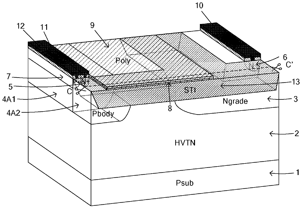
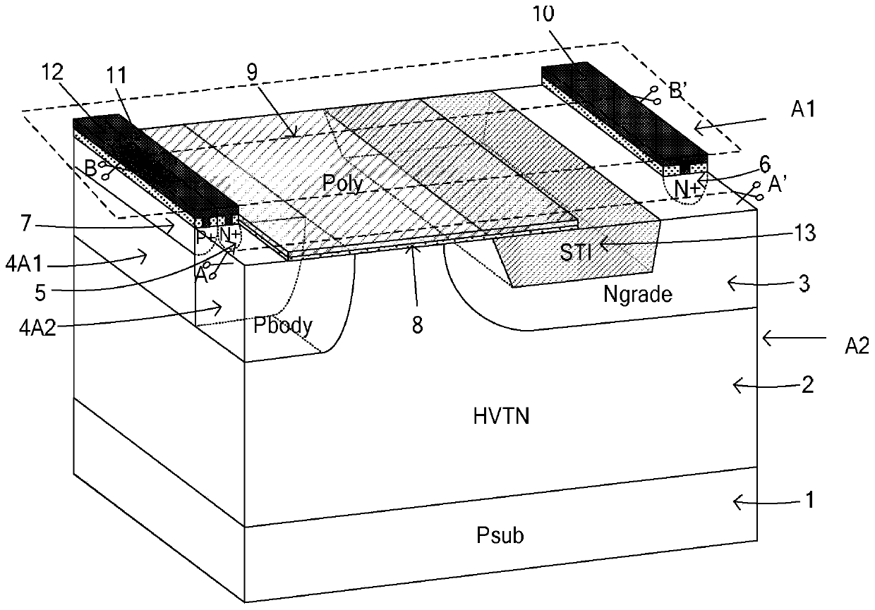
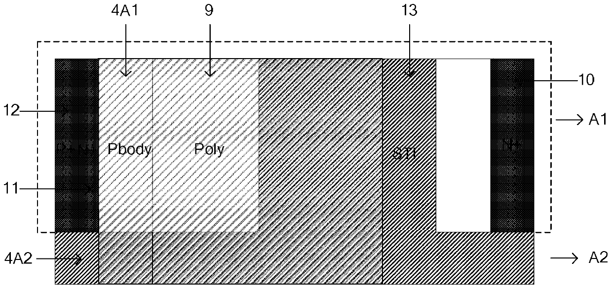
[0022] A lateral double-diffused metal oxide semiconductor device, comprising a device part A1, a terminal part A2, and a P-type substrate 1 as a device part substrate and a terminal part substrate, and a device part is arranged above the P-type substrate 1 The high-voltage N-type region 2 of the high-voltage N-type region and the terminal part of the high-voltage N-type region is provided with an N-type drift region 3 above the high-voltage N-type region 2, a P-type body region 4A1 located in the device part, and a device located in the terminal part The P-type body region 4A2 formed by diffusion of part of the P-type body region 4A1 is also provided with a gate oxide layer 8 above the high-voltage N-type region 2, and a polysilicon gate field plate 9 is provided above the gate oxide layer 8. The device part also includes a The N-type drain region 6 in the N-type drift region 3 and the N-type source region 5 and the P-type region 7 arranged in the P-type body region 4A1, in th...


PUM


Abstract

The invention relates to a lateral double-diffused metal oxide semiconductor device. The lateral double-diffused metal oxide semiconductor device comprises a device part, a terminal part and a P type substrate; a high-voltage N type region, an N type drift region, a P type body region 4A1 and a P type body region 4A2 are arranged over the P type substrate; the P type body region 4A1 is positioned in the device part; the P type body region 4A2 is positioned in the terminal part, and formed by diffusion of the P type body region 4A1 in the device part; a gate oxidization layer and a polycrystalline silicon gate field plate are also arranged over the high-voltage N type region; the device part further comprises an N type drain region, an N type source region, a P type region and a metal contact, wherein a shallow trench isolation region is arranged in the N type drift region; the shallow trench isolation region is shaped as a straight bar; the shallow trench isolation region extends to the terminal part from the device part; namely, the width of the shallow trench isolation region is the same as that of the N type drift region; and furthermore, the N type drain region, the N type source region, the P type region and the metal contact are not arranged over the P type body region 4A2 and the N type drift region of the terminal part. By means of the lateral double-diffused metal oxide semiconductor device disclosed by the invention, the breakdown voltage is improved when various performance parameters of an LDMOS device are kept same.

Description

technical field [0001] The invention relates to the technical field of power semiconductor devices, and relates to a lateral double-diffused metal oxide semiconductor device, which can be applied to the design of the terminal structure of the power semiconductor device. Background technique [0002] With the rapid development of semiconductor technology and its application fields, the manufacturing process and structure of power semiconductor devices are constantly improving, which promotes the development of power devices in the direction of high performance. [0003] Among power devices, Lateral Double-Diffused MOSFET (LDMOS for short) has the advantages of high withstand voltage, high input impedance and easy integration, so it is widely used in the manufacture of semiconductor integrated circuits. Compared with conventional MOSFETs, LDMOS devices have a low-doped drift region. When a high voltage is applied between the drain and the source, since the drift region has a ...

Claims


Application Information

Patent Timeline
Patent Type & Authority Patents(China)
IPC IPC(8): H01L29/78H01L29/06
CPCH01L29/0646H01L29/7816
Inventor 刘斯扬李胜薛颖童鑫叶然孙伟锋陆生礼时龙兴
Owner SOUTHEAST UNIV
Why Eureka
Try Eureka