Side edge coupling raster of laser and preparation method for raster, and laser comprising raster

A technology for coupling gratings and lasers, applied in the field of semiconductor technology and nanofabrication, can solve problems such as insufficient exposure and stacking, and achieve the effects of reducing costs, reducing time, and accurately and controllable exposure areas.

Active Publication Date: 2017-10-31
INST OF SEMICONDUCTORS - CHINESE ACAD OF SCI
View PDF2 Cites 2 Cited by
  • Summary
  • Abstract
  • Description
  • Claims
  • Application Information

AI Technical Summary

Problems solved by technology

The preparation of the side-coupled grating is a difficult point. This is because the ridge waveguide has a certain height and width, which is different from the planar photolithography. During the process of removing the glue, there will be glue accumulation at the bottom of the ridge. Phenomenon, for the commonly used holographic exposure, can not fully expose

Method used


Image

  • Side edge coupling raster of laser and preparation method for raster, and laser comprising raster
  • Side edge coupling raster of laser and preparation method for raster, and laser comprising raster
  • Side edge coupling raster of laser and preparation method for raster, and laser comprising raster

Examples


Embodiment Construction

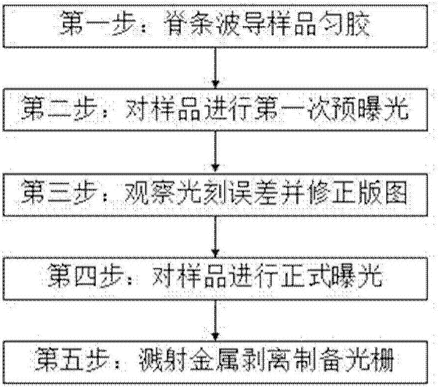
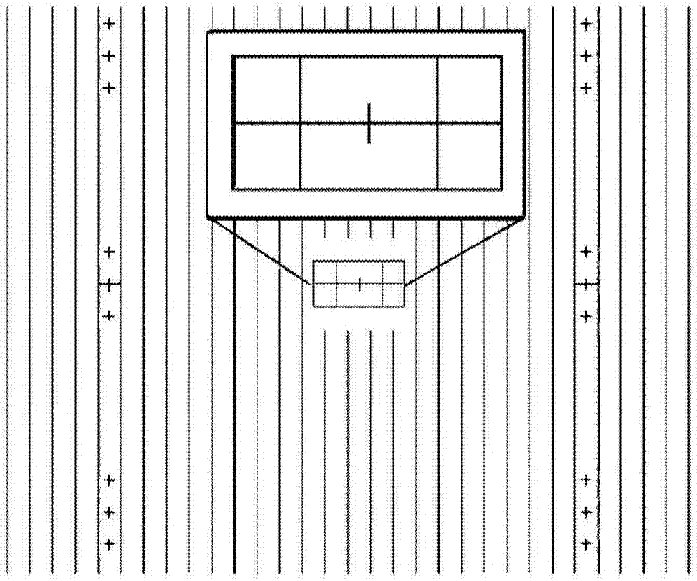
[0035] According to the general inventive concept of the present invention, a method for preparing a side coupling grating of a laser is provided, that is, the first electron beam exposure pre-lithography is performed on the epitaxial wafer carved with ridge waveguides, and then the layout and pattern are observed by SEM. The distance error of the ridge-stripe waveguide, and then correct the grating layout, perform formal grating exposure, and then perform metal sputtering and stripping to complete the preparation of the metal grating.

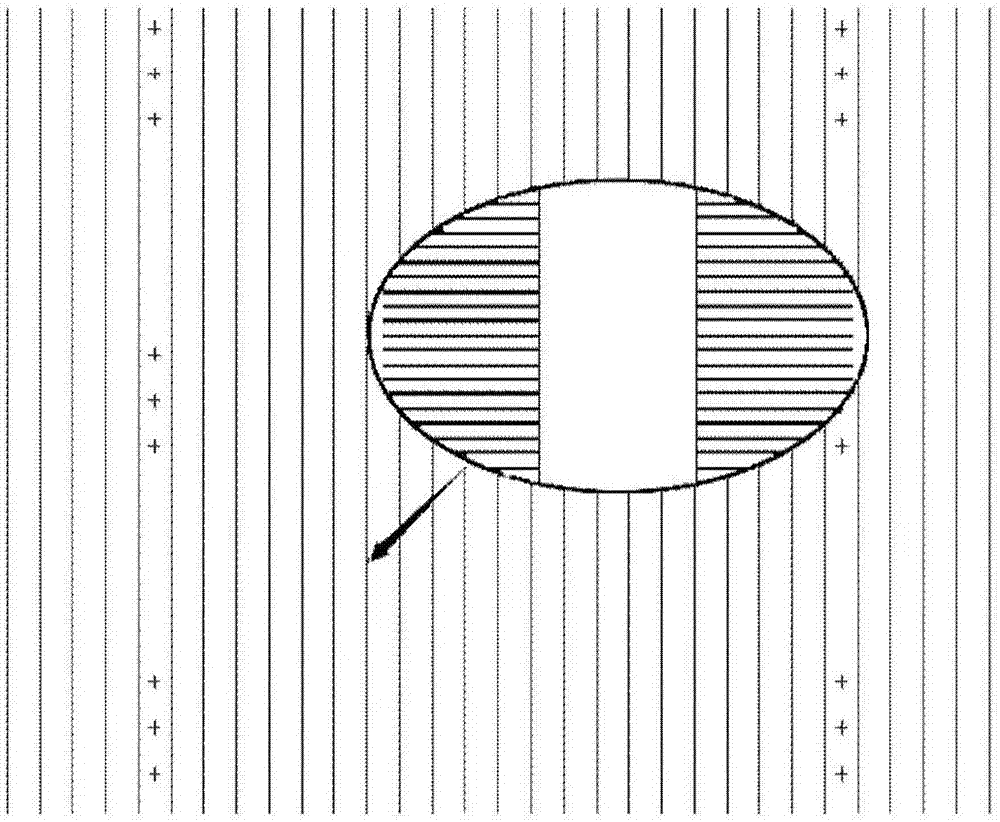
[0036] The laser ridge-stripe waveguide is formed by dry etching, preferably using an ICP etching system. Preferably, the width of the ridge-stripe waveguide is 3-5 μm. As for the position of the grating, since the distance of about 2 μm on both sides of the ridge waveguide is the effective area of ​​the grating, when designing the grating, the overall width is designed to be 2 to 3 μm on both sides of the ridge waveguide.

[0037] For the pro...


PUM


Abstract

Disclosed is a preparation method of a side edge coupling raster of a laser. The preparation method comprises the steps of 1, etching and preparing a laser ridge waveguide, preparing an electron beam lithography alignment mark on a ridge waveguide sample and coating the sample with photoresist; 2, performing primary electron beam exposure on the two sides of the ridge waveguide coated with photoresist; 3, determining distance deviation between a raster mask and the ridge waveguide after electron beam exposure, and correcting the deviation in the raster layout; 4, performing formal electron beam exposure and developing on the sample by the corrected raster layout; and 5, performing metal sputtering and striping to form the side edge coupling raster. By adoption of the preparation method, a perfect feedback raster tightly close to the ridge waveguide can be prepared, so that a good structural foundation is provided for distributed feed back die selection of the laser, electron beam exposure time is reduced, and the cost is lowered.

Description

technical field [0001] The invention relates to the field of semiconductor technology and nano-processing, and further relates to a preparation method of a side-coupled laser metal grating, a grating manufactured according to the preparation method, and a laser including the grating. Background technique [0002] Due to the advantages of small size, low cost, and easy integration, semiconductor lasers are widely used in many fields, such as space communication, gas detection, and laser countermeasures. In particular, semiconductor lasers in the mid-infrared 2-5 μm band have received more and more attention. This is because 2-5 μm is a very important atmospheric window, and the absorption characteristic lines of many gas molecules are in this band. Therefore, for atmospheric monitoring It has great application potential in civil projects such as mine gas detection and mine gas detection. Tunable DiodeLaser Atmosphere Spectrum (TDLAS for short) prepared by semiconductor lasers...

Claims


Application Information

Patent Timeline
Patent Type & Authority Applications(China)
IPC IPC(8): H01S5/12
CPCH01S5/1237
Inventor 徐云宋玉志宋甲坤张祖银陈良惠
Owner INST OF SEMICONDUCTORS - CHINESE ACAD OF SCI
Why Eureka
Try Eureka