SiC vertical double diffused metal-oxide-semiconductor (VDMOS) device and fabrication method thereof

A technology of silicon carbide and silicon carbide area, applied in semiconductor/solid-state device manufacturing, semiconductor devices, electrical components, etc., can solve problems such as rising system cost, low working speed, and increased volume

Active Publication Date: 2017-10-13
UNIV OF ELECTRONICS SCI & TECH OF CHINA
View PDF3 Cites 7 Cited by
  • Summary
  • Abstract
  • Description
  • Claims
  • Application Information

AI Technical Summary

Problems solved by technology

However, the conduction voltage drop of the parasitic silicon carbide diode obtained in this way is large (the conduction voltage drop of the silicon carbide PN junction is about 3V), and the reverse recovery characteristic is poor (the conductance modulation in the drift region injects a large amount of excess load during forward conduction flow), which leads to high power loss, which is contrary to the current application concept emphasizing green environmental protection; at the same time, because of its low working speed, it leads to low working efficiency, which is suitable for the application of silicon carbide VDMOS devices in inverter circuits, chopper circuits, etc. It is extremely unfavorable; the second is: use the device in antiparallel with an external fast recovery diode (FRD)
However, this method will cause an increase in system cost, an increase in volume, and a decrease in reliability due to the increase in metal connections, which ultimately makes the promotion of silicon carbide VDMOS devices in traditional inverter circuits, chopper circuits and other circuit applications limited. a certain obstacle
[0006] In summary, how to realize the wide application of silicon carbide VDMOS devices in inverter circuits, chopper circuits and other circuits, and solve the problems of high power loss, low work efficiency and high system cost in existing applications has become an important issue in this field. Problems that technicians need to solve urgently

Method used


Image

  • SiC vertical double diffused metal-oxide-semiconductor (VDMOS) device and fabrication method thereof
  • SiC vertical double diffused metal-oxide-semiconductor (VDMOS) device and fabrication method thereof
  • SiC vertical double diffused metal-oxide-semiconductor (VDMOS) device and fabrication method thereof

Examples


Embodiment 1

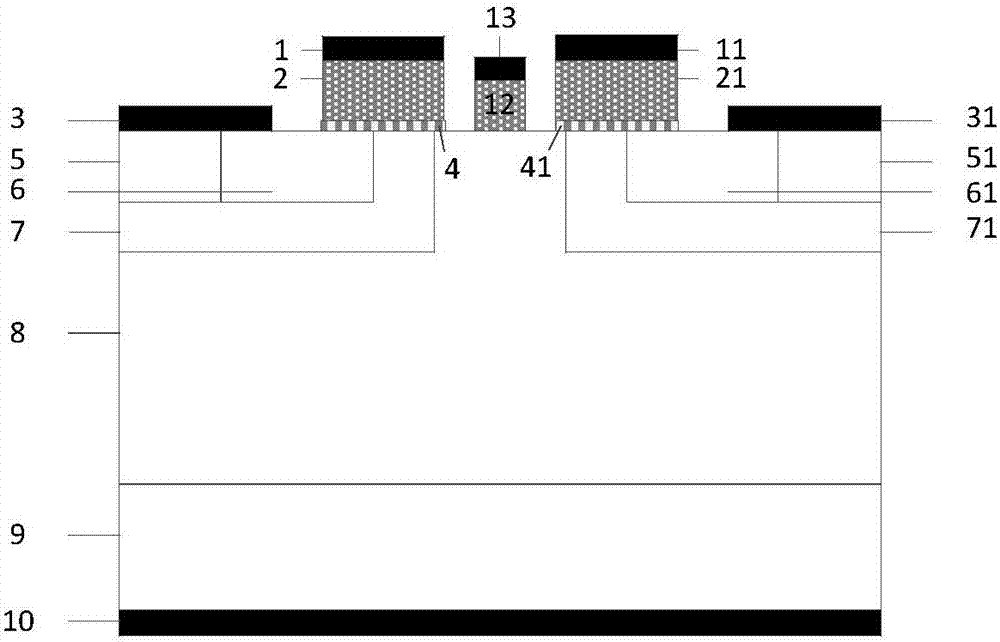
[0062] A kind of silicon carbide VDMOS device provided by the present invention, the cell structure of its basic structure is as follows figure 2 shown. It includes a metal drain electrode 10 arranged sequentially from bottom to top with a thickness of about 0.5-6 μm and a doping concentration of 1×10 18 cm -3 ~1×10 19 cm -3 , N with a thickness of 50-200 μm + The substrate 9 has a thickness of 15-18 μm and a doping concentration of about 1×10 15 cm -3 ~5×10 16 cm -3 N - Epitaxial layer 8; above the N- epitaxial layer 8 has a doping concentration of 1×10 17 ~7×10 17 cm -3 1. Implant the first Pbase region 7 with a depth of about 0.5-1 μm, and the other end of the upper layer has a second Pbase region 71 with the same parameters; the first Pbase region 7 has mutually independent doping concentrations of 1×10 19 ~1×10 20 cm -3 , implanting the first N with a depth of about 0.3-0.5 μm + The source region 6 and the doping concentration are about 3×10 19 ~1×10 20 ...

Embodiment 2

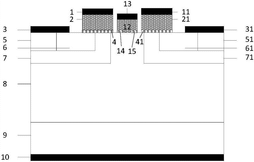
[0064] except P + Both sides below the polysilicon layer 12 also have N - The first dielectric layer 14 and the second dielectric layer 15 in direct contact with the epitaxial layer 8 are the same as the first embodiment in the rest of the structure of this embodiment.

[0065] In diode application, the first dielectric layer 14 and the second dielectric layer 15 are at P + The electron accumulation layer formed under the polysilicon layer 12 can further reduce the drift region resistance of the device, thereby reducing the forward conduction voltage drop of the device.

Embodiment 3

[0067] divide by N - In the epitaxial layer 8 and under the first Pbase region 7, there is also a first P-type silicon carbide region 16 forming a super junction or semi-super junction structure, and the N - In the epitaxial layer 8 and below the first Pbase region 7 there is also a second P-type silicon carbide region 161 forming a superjunction or semi-superjunction structure, and the rest of the structure of this embodiment is the same as that of Embodiment 1.

[0068] The formation of a superjunction or semi-superjunction structure can further reduce the drift region resistance of the device in diode applications and MOS applications, thereby reducing the forward conduction voltage drop of the device.

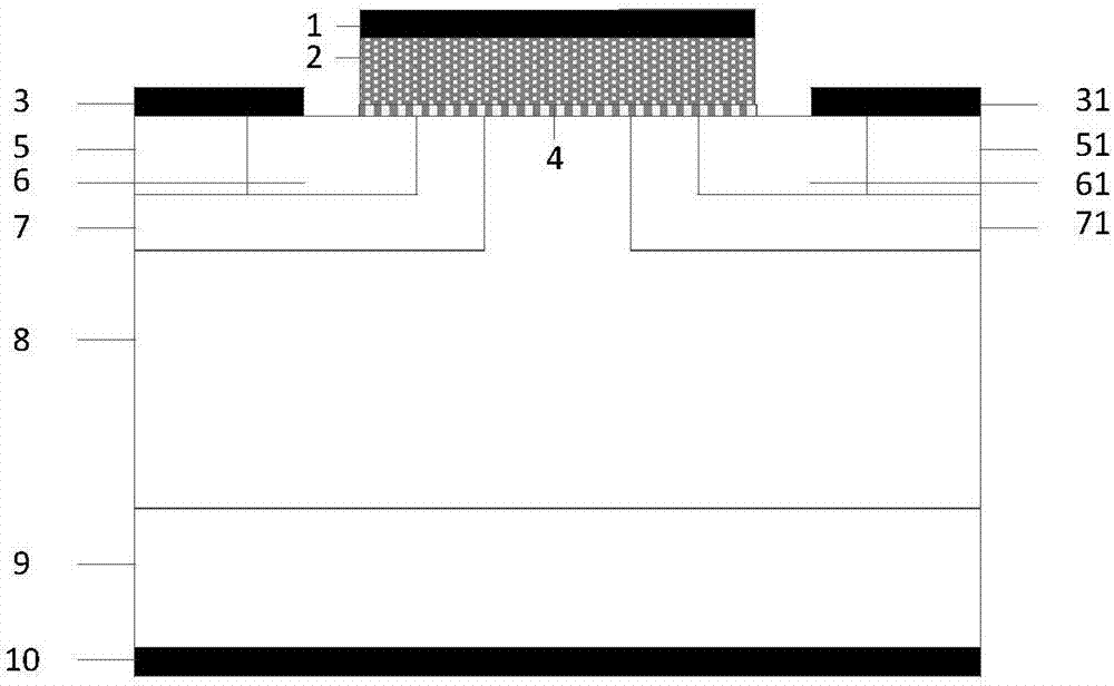
[0069] and figure 1 Compared with the cell structure of the traditional silicon carbide VDMOS device shown, the present invention deposits a polysilicon layer on the surface of the JFET region of the silicon carbide VDMOS device to form a Si / SiC heterojunction. Applicatio...


PUM


Abstract

The invention discloses a SiC vertical double diffused metal-oxide-semiconductor (VDMOS) device and a fabrication method thereof, and belongs to the technical field of a power semiconductor. A poly-silicon layer is directly deposited on a surface of a junction field-effect transistor (JFET) region of the SiC VDMOS device to form a Si / SiC heterojunction, a diode is further integrated in the device, and the application of the device in the field of an inversion circuit, a chopping circuit and the like is optimized. Compared with the prior art directly employing a VDMOS parasitic SiC diode, the SiC VDMOS device has the advantages of relatively low power loss, relatively fast working speed and relatively high working efficiency, and positive conduction is easier to achieve; compared with the prior art that a fast recovery diode (FRD) is reversely connected with the exterior of the device in parallel, the SiC VDMOS device has the advantages that the usage number of the device is reduced, connection lines between the devices are reduced, and the miniature development of the device is promoted; moreover, the grid width is reduced, the grid capacitance is reduced, and the working speed of the device is further increased; and therefore, the VDMOS device proposed by the invention has wide application prospect in the circuit field of the inversion circuit, the chopping circuit and the like.

Description

technical field [0001] The invention belongs to the technical field of power semiconductors, and in particular relates to a silicon carbide VDMOS device and a manufacturing method thereof. Background technique [0002] Since mankind entered the 21st century, energy issues have become increasingly prominent. Today, as the call for energy saving and emission reduction is getting louder and louder, the problem of electric energy conversion in household appliances, electric vehicles, industrial production, and locomotive traction is particularly important. Researchers in the field of power electronics can optimize and improve the power management system. It seems very important. [0003] Power devices are at the heart of modern power systems. Since the performance of traditional silicon-based power devices is very close to the limit of silicon materials, it is difficult to greatly improve their performance. Therefore, some wide-bandgap semiconductor materials such as silicon ...

Claims


Application Information

Patent Timeline
Patent Type & Authority Applications(China)
IPC IPC(8): H01L29/78H01L29/06H01L21/336
CPCH01L29/0611H01L29/0688H01L29/66712H01L29/7802
Inventor 张金平邹华刘竞秀李泽宏任敏张波
Owner UNIV OF ELECTRONICS SCI & TECH OF CHINA
Why Eureka
Try Eureka