rf power transistor with impedance matching circuit and its manufacturing method

A technology of circuits and terminal circuits, applied in circuits, amplifiers with semiconductor devices/discharge tubes, electric solid state devices, etc.

Active Publication Date: 2022-02-25
NXP USA INC
View PDF6 Cites 0 Cited by
  • Summary
  • Abstract
  • Description
  • Claims
  • Application Information

AI Technical Summary

Problems solved by technology

[0004] Designing RF amplifier devices with high ISBW is challenging

Method used


Image

  • rf power transistor with impedance matching circuit and its manufacturing method
  • rf power transistor with impedance matching circuit and its manufacturing method
  • rf power transistor with impedance matching circuit and its manufacturing method

Examples


Embodiment Construction

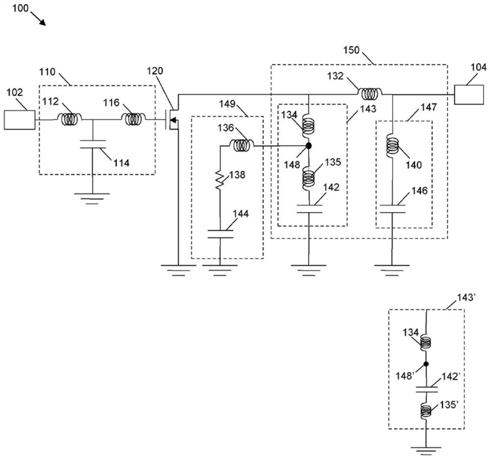
[0048] An output impedance matching circuit in a conventional RF power amplifier arrangement may include, among other things, a shunt circuit that acts as a high-pass matching stage. For example, a conventional shunt circuit may include an inductor (herein, a "shunt inductor" or L shunt ) and capacitors (herein, “shunt capacitors” or C shunt ). In conventional arrangements, the "RF cold spot" is located between the shunt inductor and the shunt capacitor. Essentially, an RF cold spot is a node that can act as a virtual ground reference voltage for RF electrical signals. If the RF cold spot were ideal, then little or no RF energy would exist at the RF cold spot at the center operating frequency of the power amplifier during device operation. However, the RF cold spot in conventional shunt circuits is not ideal, so during operation, at the center frequency, some RF energy exists at the RF cold spot.

[0049] To increase the low frequency resonance (LFR) of the device, and thu...


PUM


Abstract

An embodiment of an RF amplifier includes a transistor having a control terminal and first and second current-carrying terminals, and a shunt circuit coupled between the first current-carrying terminal and a ground reference node. The shunt circuit includes a first shunt inductor, a second shunt inductor, and a shunt capacitor coupled in series. The second shunt inductor and the shunt capacitor form a series resonant circuit near a center operating frequency of the amplifier, and an RF cold spot node exists between the first and second shunt inductors. The RF amplifier also includes a video bandwidth circuit coupled between the RF cold-spot node and the ground reference node.

Description

technical field [0001] Embodiments of the subject matter described herein relate generally to packaged semiconductor devices, and more particularly, to packaged radio frequency (RF) semiconductor devices that include impedance matching circuits. Background technique [0002] A typical high power radio frequency (RF) semiconductor device may include one or more input leads, one or more output leads, one or more transistors, bond wires coupling the input leads to the transistors, and bond wires coupling the transistors to the output leads fit line. Bond wires have significant inductance at high frequencies, and such inductance is taken into account in the design of the input and output impedance matching circuits for the device. In some cases, the input and output impedance matching circuits may be contained within the same package that contains the transistors of the device. More specifically, an in-package input impedance matching circuit may be coupled between an input le...

Claims


Application Information

Patent Timeline
Patent Type & Authority Patents(China)
IPC IPC(8): H03F1/56H03F3/19H04N5/14
CPCH03F1/56H03F3/19H04N5/147H03F2200/552H03F2200/451H03F2200/222H03F2200/225H03F3/195H03F2200/387H01L23/66H01L2223/6655H01L2224/48091H01L2224/4813H01L2224/48137H01L2224/49175H03F2200/108H03F2200/181H03F2200/297H03F2200/309H03F2200/391H03F2200/402H03F2200/75H03F1/565H03F2200/216H03F2200/301H01L2924/00014
Inventor 朱宁达蒙·G·霍尔默斯杰弗里·凯文·琼斯
Owner NXP USA INC
Why Eureka
Try Eureka