Wafer test method for memory chip with redundant cell

A memory chip and memory testing technology, which is applied to static memory and instruments, can solve the problems of long test time, high test cost, and low test efficiency, etc., to improve test efficiency, reduce test cost, and reduce reading time Effect

Active Publication Date: 2017-08-11
SHANGHAI HUAHONG GRACE SEMICON MFG CORP
View PDF8 Cites 10 Cited by
  • Summary
  • Abstract
  • Description
  • Claims
  • Application Information

AI Technical Summary

Problems solved by technology

However, this method needs to repeatedly read the BIT MAP, and then do the algorithm operation, because the reading and algorithm operation are serial operations on the bus, and the efficiency of the same test is not high. If the number of simultaneous tests is high, the test time will be very long, resulting in The cost of testing is too high, so how to reduce the test time of chips with redundant units has become a huge challenge for test engineers

Method used


Image

  • Wafer test method for memory chip with redundant cell
  • Wafer test method for memory chip with redundant cell
  • Wafer test method for memory chip with redundant cell

Examples


Embodiment Construction

[0031] Firstly, the test mechanism of the existing memory tester to test chips with redundant functions is explained as follows:

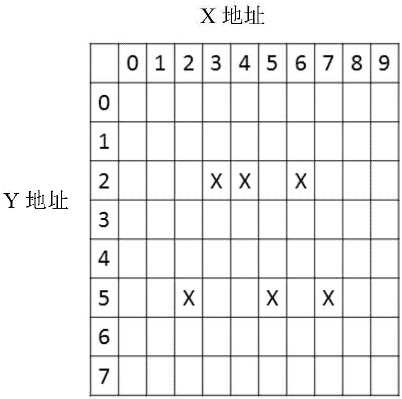
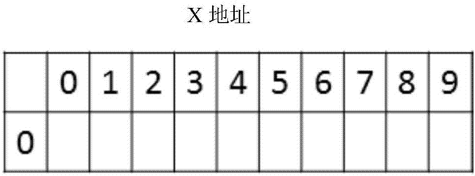
[0032] To test this type of chip, a dedicated memory tester is generally required, because the memory tester has a special RAM to store the address of the failed unit of the chip under test (DUT), generally referred to as ECR or AFM. For a simple example, such as figure 1 As shown, it is the array structure diagram of the main area of ​​the memory chip on the wafer. A certain memory chip is composed of 10 units of X address and 8 units of Y address. X address is defined as column address, and Y is defined as row address; while redundant The unit unit is one line, that is, 10 units in the X direction and 1 unit in the Y direction. For the structure diagram of redundant units, please refer to figure 2 shown. Because the smallest unit of a redundant unit is a row, as long as there is a unit failure in a row, this row is judged to be a failure and n...


PUM


Abstract

The present invention discloses a wafer test method for a memory chip with a redundant cell. The method comprises the steps of: step one. according to an array structure of a main zone and a structure of a redundant cell of a memory chip on a wafer, setting length of a line address and a column address of a memory of a memory failure address in a memory test machine; step two. testing a chip unit, and after performing an OR operation on a testing result of each line, storing the testing result into a memory of the memory failure address with a same line address; step three. reading content of each line in the memory of the memory failure address to obtain a quantity of failed line and line addresses; and step four. determining whether each failed line of the main zone of the memory chip can be restored, and if yes, allocating a redundant cell to replace the failed line of the main zone of the memory chip. The method provided by the present invention can effectively reduce testing time and reduce testing costs.

Description

technical field [0001] The invention relates to a semiconductor integrated circuit manufacturing process method, in particular to a wafer testing method for memory chips with redundant units. Background technique [0002] Wafer testing (Circuit Probing, CP), also known as circuit needle testing, is to test the chip die (die) directly on the wafer (wafer) before packaging to verify whether each chip meets the product specifications. [0003] At present, when testing the memory chip (Memory IC), in order to improve the test yield rate, the redundant unit (Redundancy Sector) will be added when the memory chip is tested on the wafer. fail bit cell), the redundant unit can be used to replace the failed unit in the main area. There are generally two replacement methods: hardware replacement and software replacement. Now the more common method is software replacement. [0004] To test this type of chip, a dedicated memory tester (Memory Tester) is generally required, because the m...

Claims


Application Information

Patent Timeline
Patent Type & Authority Applications(China)
IPC IPC(8): G11C29/00
CPCG11C29/006G11C29/702
Inventor 朱渊源
Owner SHANGHAI HUAHONG GRACE SEMICON MFG CORP
Why Eureka
Try Eureka