
Flexible circuit board and manufacturing method thereof

A flexible circuit board and manufacturing method technology, applied in the directions of printed circuits, printed circuits, printed circuit components, etc., can solve the problems of high material cost, large signal attenuation of transmission lines, large dielectric loss, etc., to reduce signal transmission loss, reduce The effect of production costs

Active Publication Date: 2017-07-21
HONGQISHENG PRECISION ELECTRONICS (QINHUANGDAO) CO LTD +2
View PDF3 Cites 3 Cited by
  • Summary
  • Abstract
  • Description
  • Claims
  • Application Information

AI Technical Summary

Problems solved by technology

However, the dielectric loss of the above materials is still relatively large, resulting in a large signal attenuation in the transmission line of the circuit board made of the above materials
In addition, Teflon and liquid crystal polymers are special materials with high material costs

Method used


Image

  • Flexible circuit board and manufacturing method thereof
  • Flexible circuit board and manufacturing method thereof
  • Flexible circuit board and manufacturing method thereof

Examples


Embodiment Construction

[0036] The flexible circuit board and the manufacturing method of the flexible circuit board provided by the present invention will be described in detail below in conjunction with specific embodiments.

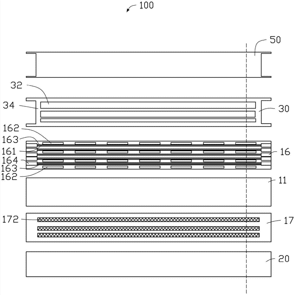
[0037] see figure 1 and figure 2 , a flexible circuit board 100 provided by the present invention, the flexible circuit board 100 includes a base layer 11, a first conductive circuit layer 16 and a second conductive circuit layer 17 formed on opposite sides of the base layer 11, formed The protective layer 20 on the second conductive circuit layer 17 , the photosensitive film 30 formed on the first conductive circuit layer 16 , and the anti-electromagnetic interference layer 50 formed on the photosensitive film 30 .

[0038] The first conductive circuit layer 16 includes at least one linear signal line 161 , at least two ground lines 162 and at least two hollow areas 163 . In this embodiment, the first conductive circuit layer 16 includes five linear signal lines 161 , fou...


PUM


Abstract

A flexible circuit board comprises a substrate layer, a first conducting circuit layer, a second conducting circuit layer, a plurality of conducting holes, a sensitive film and an anti-electromagnetic interference layer. The first conducting circuit layer and the second conducting circuit layer are formed on opposite sides of the substrate layer respectively. The plurality of conducting holes are electrically connected with the first conducting circuit layer and the second conducting circuit layer. The sensitive film is formed on the surface of the first conducting circuit layer. The anti-electromagnetic interference layer is formed on the surface of the sensitive film. The first conducting circuit layer includes at least one linear signal line, the sensitive film is provided with at least one opening, and the linear signal line is located in the opening.

Description

technical field [0001] The invention relates to a printed circuit board technology, in particular to a flexible circuit board and a method for manufacturing the flexible circuit board. Background technique [0002] In electronic signal transmission, the signal line signal attenuation of high-frequency transmission mainly comes from the attenuation caused by dielectric loss. Among them, dielectric loss is positively correlated with dielectric loss factor and relative permittivity. Traditional signal transmission structures usually use liquid crystal polymer (Liquid Crystal Polymer, LCP), Teflon (Teflon) or pure glue with low relative dielectric constant as the substrate layer covering the signal line. However, the dielectric loss of the above-mentioned materials is still relatively large, resulting in relatively large signal attenuation in the transmission line of the circuit board made of the above-mentioned materials. In addition, both Teflon and liquid crystal polymers a...

Claims


Application Information

Patent Timeline
IPC IPC(8): H05K1/02
CPCH05K1/0225H05K2201/0723
Inventor 胡先钦沈芾云何明展庄毅强
Owner HONGQISHENG PRECISION ELECTRONICS (QINHUANGDAO) CO LTD
Learn More