Electrode surface in-situ growth nano ZnO based NO2 sensor
An in-situ growth, electrode surface technology, applied in instruments, scientific instruments, material analysis by electromagnetic means, etc., can solve the problems of slow response/recovery, complex preparation process, etc., to achieve short response and recovery time, simple preparation, Solve the effect of complex preparation process
- Summary
- Abstract
- Description
- Claims
- Application Information
AI Technical Summary
Problems solved by technology
Method used
Image
Examples
Embodiment 1
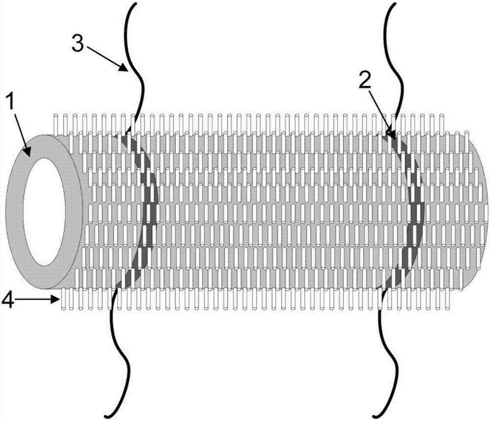
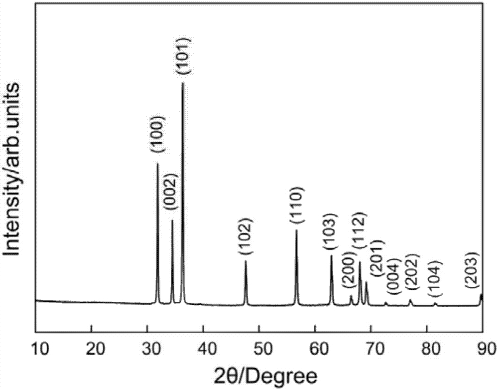
[0045] NO in situ growth of ZnO nanowire arrays on the surface of ceramic tube electrode components 2 The sensor element, its structure diagram is shown in figure 1 As shown, it consists of ceramic tubes, gold electrodes, platinum leads, and layers of gas-sensing materials. The gold electrode is covered on the surface of the ceramic tube, the platinum lead wire is welded on the surface of the gold electrode, and the gas-sensitive material is grown on the entire surface of the ceramic tube and the gold electrode. The gas-sensing material is composed of ZnO nanowire arrays, which are evenly distributed and grown on the surface of the electrode element. The ZnO nanowires have a regular shape, a smooth surface, and a single hexagonal wurtzite crystal structure, with a diameter of 80-100nm , the length is 600nm~1μm, and the aspect ratio is high.
[0046] A gas-sensing material for NO based on in-situ growth of ZnO nanowire arrays on the surface of ceramic electrodes 2 The sensor...
Embodiment 2
[0058] NO in situ growth of ZnO nanowire arrays on the surface of ceramic tube electrode components 2 The sensor element, its structure diagram is shown in figure 1 As shown, it consists of ceramic tubes, gold electrodes, platinum leads, and layers of gas-sensing materials. The gold electrode is covered on the surface of the ceramic tube, the platinum lead wire is welded on the surface of the gold electrode, and the gas-sensitive material is grown on the entire surface of the ceramic tube and the gold electrode. The gas-sensing material is composed of ZnO nanowire arrays, which are evenly distributed and grown on the surface of the electrode element. The ZnO nanowires have regular appearance, smooth surface, and a single hexagonal wurtzite crystal structure, with a diameter of 80- 100nm, length 600nm ~ 1μm, high aspect ratio.
[0059] A kind of NO based on in-situ growth of ZnO nanowire array gas-sensing material on the surface of ceramic tube electrode element 2 The sensor...
Embodiment 3
[0069] NO in situ growth of ZnO nanowire arrays on the surface of ceramic tube electrode components 2 The sensor element, its structure diagram is shown in figure 1 As shown, it consists of ceramic tubes, gold electrodes, platinum leads, and layers of gas-sensing materials. The gold electrode is covered on the surface of the ceramic tube, the platinum lead wire is welded on the surface of the gold electrode, and the gas-sensitive material is grown on the entire surface of the ceramic tube and the gold electrode. The gas-sensing material is composed of ZnO nanowire arrays, which are evenly distributed and grown on the surface of the electrode element. The ZnO nanowires have regular appearance, smooth surface, and a single hexagonal wurtzite crystal structure, with a diameter of 80- 100nm, length 600nm ~ 1μm, high aspect ratio.
[0070] A kind of NO based on in-situ growth of ZnO nanowire array gas-sensing material on the surface of ceramic tube electrode element 2 The sensor...
PUM
| Property | Measurement | Unit |
|---|---|---|
| diameter | aaaaa | aaaaa |
| length | aaaaa | aaaaa |
| length | aaaaa | aaaaa |
Abstract
Description
Claims
Application Information
 - R&D
- Intellectual Property
- Life Sciences
- Materials
- Tech Scout
- Unparalleled Data Quality
- Higher Quality Content
- 60% Fewer Hallucinations
Browse by: Latest US Patents, China's latest patents, Technical Efficacy Thesaurus, Application Domain, Technology Topic, Popular Technical Reports.
© 2025 PatSnap. All rights reserved.Legal|Privacy policy|Modern Slavery Act Transparency Statement|Sitemap|About US| Contact US: help@patsnap.com


