Silicon carbide substrate structure with trench array and cavity
A silicon carbide substrate and array technology, applied in electrical components, circuits, semiconductor devices, etc., can solve difficult problems such as silicon carbide substrate thinning process, so as to alleviate thermal stress problems, reduce substrate resistance, and debris The effect of reducing the chance of
- Summary
- Abstract
- Description
- Claims
- Application Information
AI Technical Summary
Problems solved by technology
Method used
Image
Examples
Embodiment 1
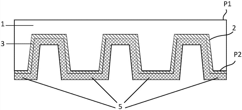
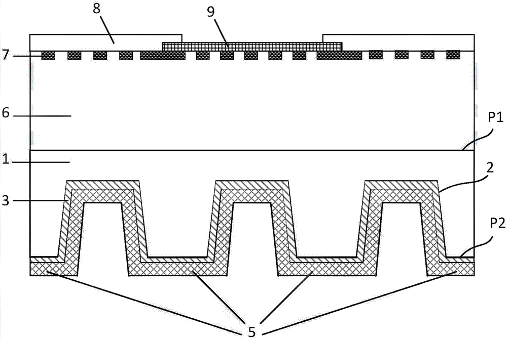
[0047] figure 2 is a schematic cross-sectional view of a silicon carbide junction barrier Schottky diode, wherein the diode adopts the substrate structure provided by the present invention. It includes a silicon carbide substrate 1, which is an N-type silicon carbide material in this embodiment; the top surface of the substrate P1; the bottom surface of the substrate P2; the trench array 2; the first layer of metal 3; the second layer of metal 5; silicon carbide epitaxy Layer 6, which is N-type semiconductor in this embodiment; heavily doped region 7, which is P-type semiconductor in this embodiment; passivation layer 8; Schottky barrier metal 9.
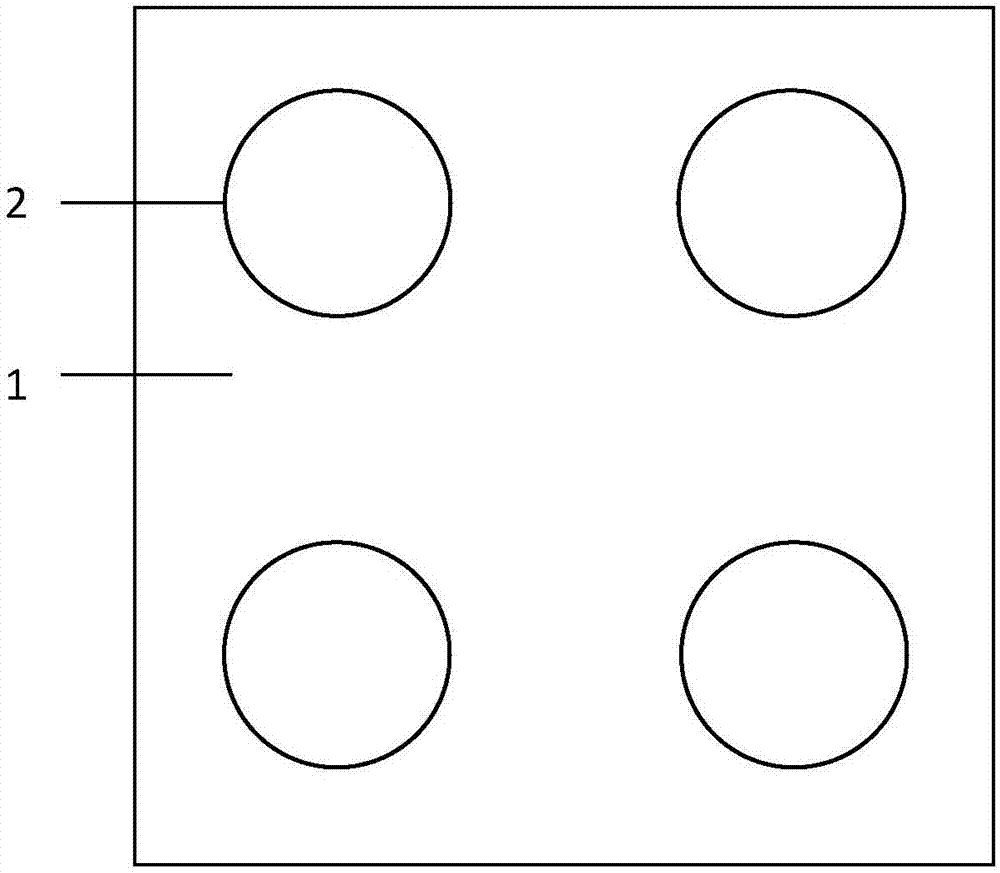
[0048] image 3 is the bottom view of the device after the trench array has been etched. In this embodiment, all the trenches are distributed in a grid pattern, and the trenches in each row are in the same column position. In this embodiment, the groove array occupies nearly 1 / 5 of the total area of the substrate bottom surfac...
Embodiment 2
[0063] figure 2 is a schematic cross-sectional view of a silicon carbide junction barrier diode, wherein the diode adopts the substrate structure provided by the present invention. Including silicon carbide substrate 1, in this embodiment is N-type silicon carbide material; substrate top surface P1; substrate bottom surface P2; trench array 2; ohmic contact layer metal 3; solder layer metal 5; silicon carbide epitaxial layer 6, N-type semiconductor in this embodiment; heavily doped region 7, P-type semiconductor in this embodiment; passivation layer 8; Schottky barrier metal 9.
[0064] Figure 4 is the bottom view of the device after the trench array has been etched. In this embodiment, all the trenches are distributed in a grid pattern, and the column positions of the trenches in two adjacent rows are staggered. In this embodiment, the groove array occupies nearly 1 / 5 of the total area of the substrate bottom surface P2.
[0065] A possible manufacturing process of th...
Embodiment 3
[0073] figure 2 is a schematic cross-sectional view of a silicon carbide junction barrier diode, wherein the diode adopts the substrate structure provided by the present invention. Including silicon carbide substrate 1, in this embodiment is N-type silicon carbide material; substrate top surface P1; substrate bottom surface P2; trench array 2; ohmic contact layer metal 3; solder layer metal 5; silicon carbide epitaxial layer 6, N-type semiconductor in this embodiment; heavily doped region 7, P-type semiconductor in this embodiment; passivation layer 8; Schottky barrier metal 9.
[0074] Figure 5 is the bottom view of the device after the trench array has been etched. In this embodiment, all the grooves are distributed in a honeycomb shape. In this embodiment, the groove array occupies nearly 1 / 5 of the total area of the substrate bottom surface P2.
[0075] A manufacturing process that can be used for the device includes the following steps.
[0076] In the first step...
PUM
| Property | Measurement | Unit |
|---|---|---|
| thickness | aaaaa | aaaaa |
| thickness | aaaaa | aaaaa |
| thickness | aaaaa | aaaaa |
Abstract
Description
Claims
Application Information
 - R&D
- Intellectual Property
- Life Sciences
- Materials
- Tech Scout
- Unparalleled Data Quality
- Higher Quality Content
- 60% Fewer Hallucinations
Browse by: Latest US Patents, China's latest patents, Technical Efficacy Thesaurus, Application Domain, Technology Topic, Popular Technical Reports.
© 2025 PatSnap. All rights reserved.Legal|Privacy policy|Modern Slavery Act Transparency Statement|Sitemap|About US| Contact US: help@patsnap.com


