Thin film transistor and preparation method thereof and array substrate
A technology of thin film transistors and semiconductors, applied in the direction of transistors, semiconductor/solid-state device manufacturing, semiconductor devices, etc., can solve the problem of low mobility, achieve the effects of simplifying the process, saving costs, and improving device mobility and stability
- Summary
- Abstract
- Description
- Claims
- Application Information
AI Technical Summary
Problems solved by technology
Method used
Image

Examples
preparation example Construction
[0054] The embodiment of the present invention also provides a method for preparing a thin film transistor, including:
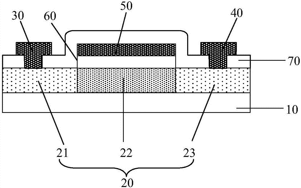
[0055] S10, such as Figure 4 As shown, a first metal layer is formed on the substrate 10, and the active region to be formed on the first metal layer is oxidized so that the material to be formed in the active region is a semiconductor, and the active layer 20 is formed.
[0056] Wherein, after the active region to be formed of the first metal layer is oxidized, the part oxidized to semiconductor on the first metal layer is used as the active region 23 of the active layer 20, and the part that is not oxidized is used as the active layer 20 source region 21 and drain region 22 .
[0057] Here, the manner of the oxidation treatment is not limited, as long as the active region to be formed of the first metal layer can be completely oxidized.
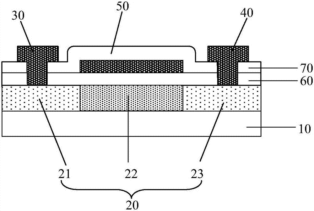
[0058] S20, such as Figure 2(a)-2(d) As shown, a gate insulating layer 60 , a gate 50 , a source 30 and a drain 40...
Embodiment 1
[0064] A method for preparing a thin film transistor is provided, such as Figure 5 As shown, it specifically includes the following steps:
[0065] S100 , as shown in FIG. 6( a ), forming a first metal layer 24 on the substrate 10 .
[0066] As an example, a photoresist layer having the first metal thin film and covering the first metal thin film can be sequentially formed on the substrate 10. After exposing and developing the photoresist layer, the photoresist can be completely reserved and partially covered to be A region with a pattern of the first metal layer is formed. Then, the first metal layer 24 is formed by etching the first metal film.
[0067] Among them, the first metal film with a thickness of 20nm-100nm can be formed by methods such as magnetron sputtering, DC sputtering, and evaporation, and its material can be indium, zinc, tin, copper, nickel, titanium, tungsten, Indium tin, indium zinc, zinc tin, indium zinc tin, etc.
[0068] S110 , as shown in FIG. 6(...
Embodiment 2
[0083] A method for preparing a thin film transistor is provided, such as Figure 7 As shown, it specifically includes the following steps:
[0084] S200 , as shown in FIG. 8( a ), form the stacked first metal layer 24 and the second metal layer 81 on the substrate 10 through the same patterning process.
[0085] Among them, the first metal layer with a thickness of 20nm-100nm can be formed by magnetron sputtering, DC sputtering, evaporation and other methods, and its material can be indium, zinc, tin, copper, nickel, titanium, tungsten, indium tin , indium zinc, zinc tin, indium zinc tin, etc.
[0086] The second metal layer with a thickness of 100nm-200nm can be formed by the same process, and its material can be Al, Ti, Ta, Hf, Zr, etc.
[0087] S210, as shown in FIG. 8(b), perform oxidation treatment on the to-be-formed active region on the first metal layer 24 and the to-be-formed gate insulating layer on the second metal layer 81, so that the to-be-formed active region...
PUM
 Abstract
Description
Claims
Application Information
 - Generate Ideas
- Intellectual Property
- Life Sciences
- Materials
- Tech Scout
- Unparalleled Data Quality
- Higher Quality Content
- 60% Fewer Hallucinations
Browse by: Latest US Patents, China's latest patents, Technical Efficacy Thesaurus, Application Domain, Technology Topic, Popular Technical Reports.
© 2025 PatSnap. All rights reserved.Legal|Privacy policy|Modern Slavery Act Transparency Statement|Sitemap|About US| Contact US: help@patsnap.com