Self-heating measuring structure and measuring method for FinFET device, and electronic device

A self-heating and device technology, used in measurement devices, semiconductor/solid-state device testing/measurement, electrical measurement, etc., can solve the problems of reduced driving current, poor heat dissipation performance of fins, and difficult detection of self-heating effects.

Active Publication Date: 2017-06-30
SEMICON MFG INT (SHANGHAI) CORP +1
View PDF2 Cites 0 Cited by
  • Summary
  • Abstract
  • Description
  • Claims
  • Application Information

AI Technical Summary

Problems solved by technology

[0004] With the continuous shrinking of the size of semiconductor devices, 3D devices face many challenges, wherein the fins have poor heat dissipation performance due to the narrow structure of the fins, which causes serious self-heating effects of FinFET devices, and the heating effect seriously affects Due to the reduction of device performance and charge carrier induced lattice vibrations (charge carrier induced lattice vibrations), the heating effect increases the temperature of the device and reduces the drive current, but for FinFET devices, the self-heating effect hard to detect

Method used


Image

  • Self-heating measuring structure and measuring method for FinFET device, and electronic device
  • Self-heating measuring structure and measuring method for FinFET device, and electronic device
  • Self-heating measuring structure and measuring method for FinFET device, and electronic device

Examples


Embodiment 1

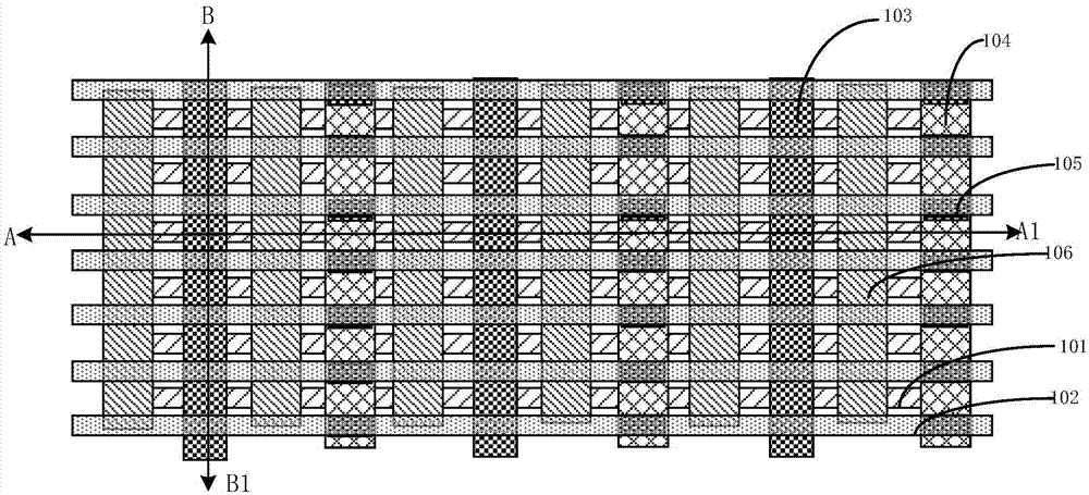
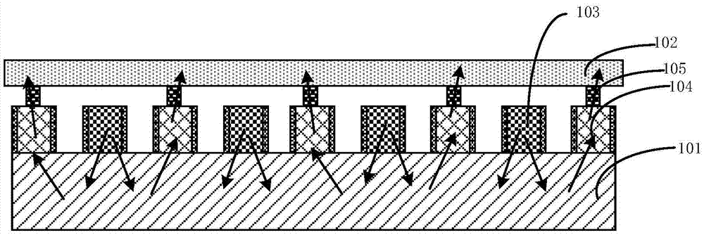
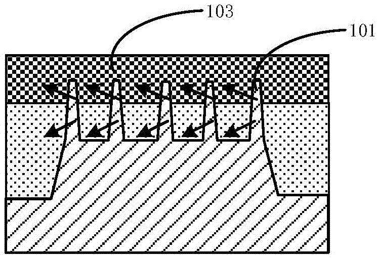
[0037] In order to solve the problems in the prior art, the present invention provides a self-heating measurement structure in a FinFET device. The measurement structure will be further described below in conjunction with the accompanying drawings, wherein figure 1 It is a schematic diagram of the self-heating measurement structure in the FinFET device described in the embodiment of the present invention; figure 2 It is a schematic cross-sectional view along A-A1 of the self-heating measurement structure in the FinFET device described in the embodiment of the present invention; image 3 It is a schematic cross-sectional view along B-B1 of the self-heating measurement structure in the FinFET device described in the embodiment of the present invention.

[0038] Such as Figure 1-3 As shown, the self-heating measurement structure includes:

[0039] semiconductor substrate;

[0040] Several rows of fins 101 are located on the semiconductor substrate;

[0041] A grid array, lo...

Embodiment 2

[0068] In order to solve the problems existing in the prior art, the present invention provides a method for measuring resistance in a FinFET device, including:

[0069] Step S1: Disconnect the FinFET device, so that the gate is in an off state, and measure the resistance value R of the thermal variable resistance layer 0 ;

[0070] Step S2: Turn on the FinFET device, so that the gate is in a conduction state, at this time, the gate will emit heat, and the heat will be transmitted to the thermal variable resistance layer along the dummy gate, as Figure 2-3 As shown, the resistance of the thermal variable resistance layer changes, and the resistance value R of the thermal variable resistance layer is measured;

[0071] Step S3: Calculate the temperature of the thermal variable resistance layer after the temperature rise according to the increase of the resistance of the thermal variable resistance layer and the temperature coefficient of resistance α.

[0072] Optionally, th...

Embodiment 3

[0080] The present invention also provides an electronic device, including the test structure described in the first embodiment.

[0081] The electronic device of this embodiment can be any electronic product or equipment such as mobile phone, tablet computer, notebook computer, netbook, game console, TV set, VCD, DVD, navigator, camera, video recorder, voice recorder, MP3, MP4, PSP, etc. , can also be any intermediate product that includes the test structure. The electronic device of the embodiment of the present invention has better performance due to the use of the above test structure.


PUM


Abstract

The invention relates to a self-heating measuring structure and measuring method for an FinFET device, and an electronic device. The self-heating measuring method for the FinFET device comprises a step S1 of switching off the FinFET device in order to make the grid be in an open circuit state, and measuring the resistance value R0 of thermal variable resistance layers; step S2 of switching on the FinFET device in order to make the grid be in a conduction state, and measuring the resistance value R of the thermal variable resistance layers; and a step S3 of calculating the temperature of the thermal variable resistance layers after the temperature is increased in dependence on the increase of the resistance of the thermal variable resistance layers and the resistance temperature coefficient [alpha]. In the measuring structure, virtual grids are arranged among grids, and several rows of the thermal variable resistance layers connected with the virtual grids through a heat conduction material are arranged above a grid array, heat radiated from the grids are transmitted to the thermal variable resistance layers through the virtual grids, after the temperature of the thermal variable resistance layers is changed, the resistance is changed, and detection of the self-heating condition of the FinFET device is achieved by measuring the resistance of the thermal variable resistance layers.

Description

technical field [0001] The invention relates to the field of semiconductors, in particular, the invention relates to a FinFET device self-heating measurement structure, a measurement method, and an electronic device. Background technique [0002] With the continuous development of semiconductor technology, in order to improve the performance of the device, the size of integrated circuit devices needs to be continuously reduced. With the continuous reduction of the size of CMOS devices, the development of three-dimensional designs such as fin field effect transistors (FinFET) has been promoted. [0003] Compared with the existing planar transistors, the FinFET device has superior performance in terms of channel control and short channel effect reduction; the planar gate structure is arranged above the channel, and the gate in the FinFET The fins are arranged around the fins, so static electricity can be controlled from three sides, and the performance in static electricity co...

Claims


Application Information

Patent Timeline
Patent Type & Authority Applications(China)
IPC IPC(8): H01L23/544G01R31/26
CPCH01L22/34G01R31/26G01R31/2644
Inventor 周飞
Owner SEMICON MFG INT (SHANGHAI) CORP
Why Eureka
Try Eureka