Miniature ultra-wide-band antenna

An ultra-wideband antenna and antenna technology, applied in the direction of antenna, antenna grounding device, antenna grounding switch structure connection, etc., can solve the problems of reduced antenna resonance frequency, small technical application occasions, increased equipment volume, etc., to save size and overall space. Compact structure and the effect of meeting phase requirements

Active Publication Date: 2017-06-20
UNIV OF ELECTRONICS SCI & TECH OF CHINA
View PDF1 Cites 9 Cited by
  • Summary
  • Abstract
  • Description
  • Claims
  • Application Information

AI Technical Summary

Problems solved by technology

Due to the high requirements on the position of the short-circuit probe due to the impedance matching characteristics, it will add great difficulties to the manufacturing process, and this technology is used in a small number of occasions
The third method is not only complex in structure, but also the addition of active structures will virtually increase the volume of the device
The article "A miniaturized antipodal Vivaldi antenna with improved radiation characteristics" published in 2011 uses a tapered slotting technique, but the improved antenna size is 0.4λ 0 X0.69λ 0 (λ 0 is the wavelength corresponding to the lowest resonance frequency) is still relatively large, and the article "ANovel Miniaturized Vivaldi Antenna Using Tapered Slot Edge with ResonantCavity Structure for Ultra-wide Band Applications" published in 2015 has been improved on the basis of the previous literature, adding A pair of resonant cavities further reduce the resonant frequency of the antenna, and the size is reduced to 0.25λ 0 ×0.43λ 0 However, there are some shortcomings in this method. Impedance matching has relatively high requirements on the size and position of the resonant cavity, and the original antenna structure must have enough reserved space to realize this function, so that its length cannot be further shortened.

Method used


Image

  • Miniature ultra-wide-band antenna
  • Miniature ultra-wide-band antenna
  • Miniature ultra-wide-band antenna

Examples


Embodiment Construction

[0026] Embodiments of the present invention are described below through specific examples, and those skilled in the art can easily understand other advantages and effects of the present invention from the content disclosed in this specification. The present invention can also be implemented or applied through other different specific implementation modes, and various modifications or changes can be made to the details in this specification based on different viewpoints and applications without departing from the spirit of the present invention.

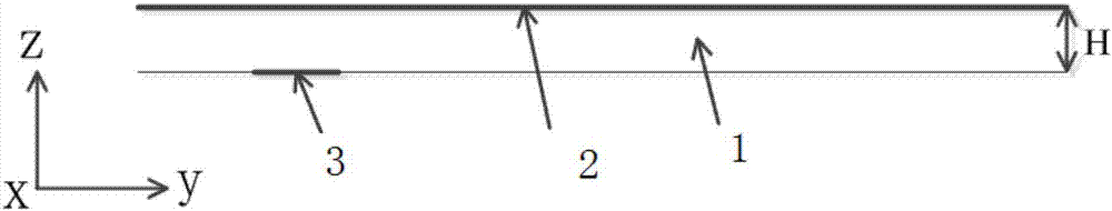
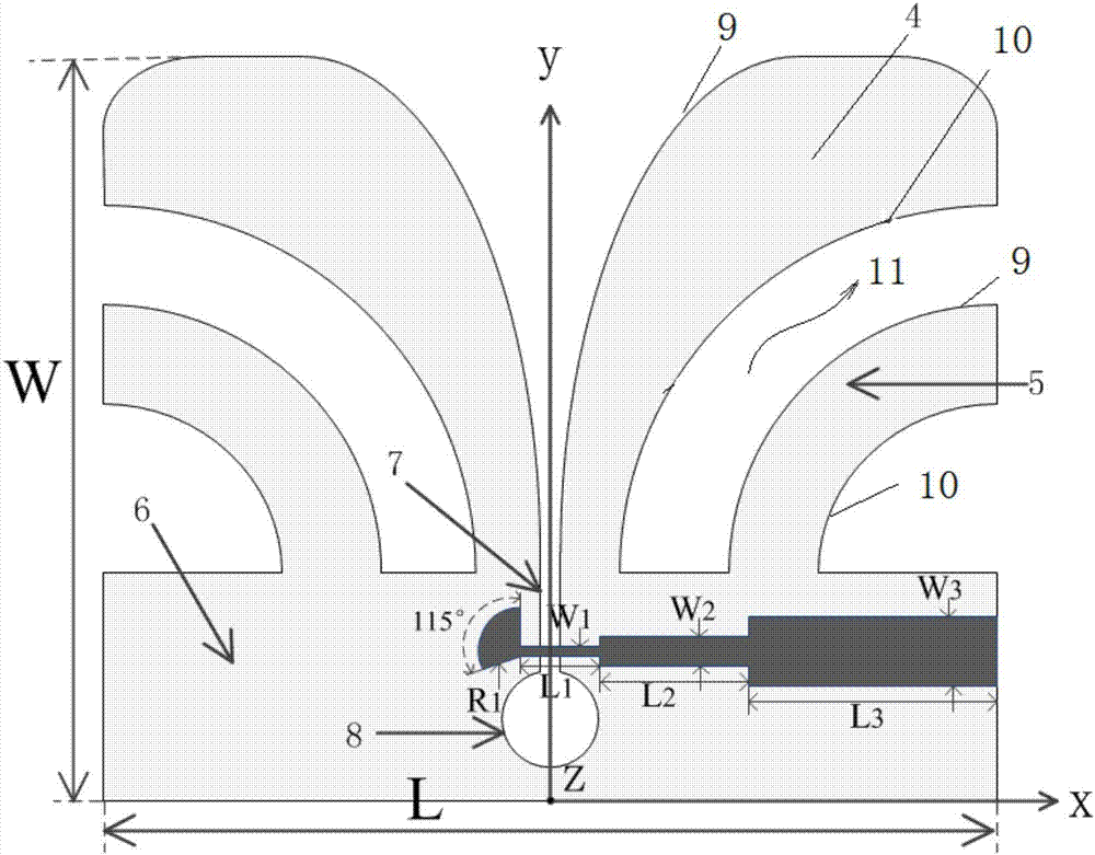
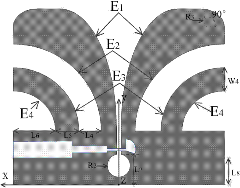
[0027] A miniaturized ultra-wideband antenna. This embodiment adopts a planar printed antenna, including a dielectric substrate 1. The dielectric substrate 1 adopts an FR4 plate with a dielectric constant of 4.4. The upper and lower surfaces of the dielectric substrate are respectively covered with metal patches. The metal stickers on the upper surface The chip is an antenna patch 2, and the metal patch on the lower surface is a micros...


PUM


Abstract

The invention provides a miniature ultra-wide-band antenna. The miniature ultra-wide-band antenna comprises a dielectric substrate and metal patches on the upper surface and the lower surface of the dielectric substrate, wherein the metal patch on the upper surface is an antenna patch, and the metal path on the lower surface is a microstrip feeder; the antenna patch comprises an earth plate, a short branch knot and a long branch knot, each of the long branch shot and the short branch shot comprises an internal slot line and an external slot line, the center of the earth plate is provided with a vertically slotted slot line, the upper part of the slotted line is connected to the internal slot line of the long branch knot, the bottom of the slotted line is connected to a circular slot, the edge shapes of the external slotted lines and the internal slotted lines of the long branch knot and the short branch knot adopt exponential type transition curves, and an exponential annular slot is formed between an external slot of the long branch knot and an internal slot of the short branch knot. The overall space of the miniature ultra-wide-band antenna is compact in structure, an antenna backboard is tightly connected with the feeder, a radiation element saves the dimensions while meeting a phase-position requirement in virtue of a coplanar strip line coupling power supply manner, the design is convenient, the principle that the antenna is additionally provided with the exponential annular slot to transfer the radiation of low-frequency points is easy to understand, and the replicability of a miniature scheme is high.

Description

technical field [0001] The invention relates to the technical field of miniaturization of planar printed microstrip antennas, in particular to how to realize miniaturization of an ultra-wideband antenna by adding an exponential annular groove structure without affecting the radiation performance of the original main structure. Background technique [0002] With the great development of wireless communication technology, people have higher and higher requirements on the portability of wireless communication equipment, which prompts the development of wireless communication equipment in the direction of miniaturization. [0003] So far, there are four main methods in the industry to solve the above problems: one is to use a dielectric board with a high dielectric constant. The second is loading short-circuit probes, the third is active structure, and the fourth is slotting and slotting technology. The idea of ​​the first method is simple and clear. When the resonant frequency...

Claims


Application Information

Patent Timeline
IPC IPC(8): H01Q1/38H01Q1/48H01Q1/50H01Q5/10H01Q5/307
CPCH01Q1/38H01Q1/48H01Q1/50H01Q5/10H01Q5/307
Inventor 杨德强耿东东肖花王清松曹飞飞杨天明孙凯胡鉴中
Owner UNIV OF ELECTRONICS SCI & TECH OF CHINA
Why Eureka
Try Eureka