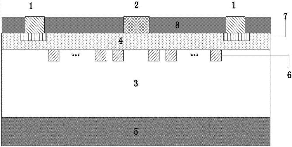
High-breakdown-voltage Schottky diode and making method
A Schottky diode, high breakdown voltage technology, applied in the field of microelectronics, can solve problems such as increased parasitic capacitance and enhanced parasitic effect
- Summary
- Abstract
- Description
- Claims
- Application Information
AI Technical Summary
Problems solved by technology
Method used
Image
Examples
Embodiment 1
[0035] Example 1, the substrate is sapphire, 12 H with a width of 2 μm and a depth of 20 μm + Injection area, H + The spacing between implanted regions is sequentially increased to 0.5 μm for Schottky diodes.
[0036] Step 1, wash the sample.
[0037] 1a) For Ga that has been grown epitaxially on the substrate 2 o 3 The sample of the layer was organically cleaned, ultrasonicated with acetone for 5 minutes, ethanol for 5 minutes, and then washed with flowing deionized water, in which the epitaxially grown Ga 2 o 3 The layer consists of two layers, the first layer has a carrier concentration of 10 14 cm -3 , Ga with a thickness of 1.5 μm 2 o 3 epitaxial layer, the second layer has a carrier concentration of 10 17 cm -3 , low-doped n-type Ga with a thickness of 130nm 2 o 3 film;
[0038] 1b) Chemical cleaning
[0039] Place the organically cleaned samples in HF:H 2 Corrode in O=1:1 solution for 30s, then wash with flowing deionized water and blow dry with high-puri...
Embodiment 2
[0070] Embodiment 2, making substrate is Ga 2 o 3 , 10 H with a width of 2.5 μm and a depth of 35 μm + Injection area, H + The spacing between the implanted regions was sequentially increased to 0.7 μm for Schottky diodes.
[0071] Step one, wash the sample.
[0072] 1.1) For Ga that has been epitaxially grown on the substrate 2 o 3 Layer samples were sonicated with acetone for 5 minutes, ethanol for 5 minutes, and then washed with flowing deionized water, in which the epitaxially grown Ga 2 o 3 The layer consists of two layers, the first layer has a carrier concentration of 10 15 cm -3 , Ga with a thickness of 1.3 μm 2 o 3 epitaxial layer, the second layer has a carrier concentration of 5×10 17 cm -3 , low-doped n-type Ga with a thickness of 110nm 2 o 3 film;
[0073] 1.2) Chemical cleaning
[0074] Step 1b) in Example 1 of this step is the same.
[0075] Step 2, depositing SiO with a thickness of 50nm 2 mask.
[0076] Put the dried sample into PECVD equipm...
Embodiment 3
[0103] Embodiment 3, making substrate is MgAl 2 o 4 , eight H with a width of 3 μm and a depth of 50 μm + Injection area, H + The spacing between the implanted regions was sequentially increased to 1.0 μm for Schottky diodes.
[0104] Step A, wash the sample.
[0105] A1) For Ga that has been epitaxially grown on the substrate 2 o 3 Layer samples were sonicated with acetone for 5 minutes, ethanol for 5 minutes, and then washed with flowing deionized water, in which the epitaxially grown Ga 2 o 3 The layer consists of two layers, the first layer has a carrier concentration of 10 16 cm -3 , Ga with a thickness of 1 μm 2 o 3 epitaxial layer, the second layer has a carrier concentration of 10 18 cm -3 , low-doped n-type Ga with a thickness of 100nm 2 o 3 film;
[0106] A2) Chemical cleaning
[0107] This step is the same as step 1b) in Example 1.
[0108] Step B, depositing SiO with a thickness of 50nm 2 mask.
[0109] Put the dried sample into PECVD equipment t...
PUM
 Abstract
Description
Claims
Application Information
 - R&D
- Intellectual Property
- Life Sciences
- Materials
- Tech Scout
- Unparalleled Data Quality
- Higher Quality Content
- 60% Fewer Hallucinations
Browse by: Latest US Patents, China's latest patents, Technical Efficacy Thesaurus, Application Domain, Technology Topic, Popular Technical Reports.
© 2025 PatSnap. All rights reserved.Legal|Privacy policy|Modern Slavery Act Transparency Statement|Sitemap|About US| Contact US: help@patsnap.com


