Thermal field structure for supersized silicon ingot

A super-sized silicon ingot technology, applied in the field of polysilicon production equipment, can solve problems such as the inability to effectively reduce crystal dislocations and impurities, unfavorable growth of super-large silicon ingots, and unsatisfactory temperature gradients, so as to improve process flexibility and save The effect of using cost and expanding the internal size

Pending Publication Date: 2017-06-20
连云港清友新能源科技有限公司
View PDF6 Cites 1 Cited by
  • Summary
  • Abstract
  • Description
  • Claims
  • Application Information

AI Technical Summary

Problems solved by technology

[0004] The polycrystalline silicon ingots on the market mainly include: the weight is about 450kg, and 5*5=25 small square ingots of G5 silicon ingots can be squared; the weight is about 850kg, and 6*6=36 small square ingots of G6 silicon ingots can be squared. The weight of upper silicon ingot is small, the productivity is low, the unit consumption is high, and the cost is high
[0005] Most of the polycrystalline ingot furnaces on the market are equipped with heating methods: upper and lower heating, and 5-side heating. At the same time, the design of the thermal field structure and the crystallization control device are not conducive to the growth of super-sized silicon ingots, which is reflected in the unsatisfactory temperature gradient. , the solid-liquid interface of the long crystal is obviously convex and concave, which cannot effectively reduce the dislocation and impurity removal in the crystal, reduce the grain boundary or make the grain uniform, etc., which has a great impact on the overall quality of the crystal, and the quality is average

Method used


Image

  • Thermal field structure for supersized silicon ingot
  • Thermal field structure for supersized silicon ingot
  • Thermal field structure for supersized silicon ingot

Examples


Embodiment Construction

[0027] The specific technical solutions of the present invention will be further described below with reference to the accompanying drawings, so that those skilled in the art can further understand the present invention, without limiting their rights.

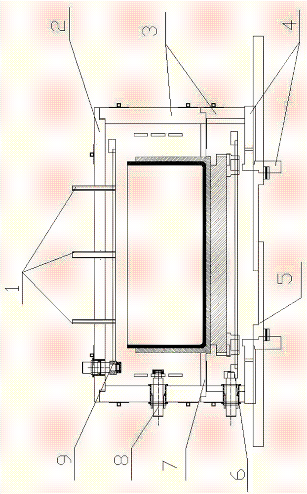
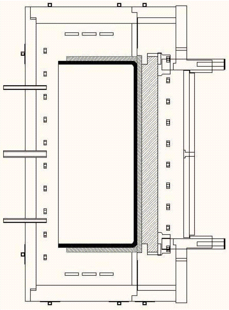
[0028] refer to figure 1 and figure 2 , a thermal field structure for super-sized silicon ingots, including a heat insulation cage surrounded by a top heat preservation component 2, a side heat preservation component 3 and a bottom heat preservation component 4. The size of the heat insulation cage is designed according to the size of the crucible. A heat exchange control device 5 is provided at the bottom of the heat-insulation cage, and a directional solidified block for placing a graphite crucible is arranged in the heat-insulated cage above the heat-exchange control device 5. The directional solidified block is used to support the crucible and is used for crystallization simultaneously. Heat exchange, can assist heat cond...


PUM


Abstract

The invention relates to a thermal field structure for a supersized silicon ingot. The thermal field structure comprises a heat insulating cage enclosed by a top heat insulating component 2, a side heat insulating component 3 and a bottom heat insulating component 4, wherein a heat exchange control device 5 is arranged at the bottom of the heat insulating cage; a directional solidification block for putting a graphite crucible is arranged in the heat insulating cage above the heat exchange device 5; a hot area separating board 7 is arranged between the periphery of the bottom of the graphite crucible and the side heat insulating component; 1 to 6 air inlet pipes are arranged on the top heat insulating component 2; a top heating electrode is arranged on the top heat insulating component 2; a side heating electrode and a bottom heating electrode are arranged on the side heat insulating component 3. According to the thermal field structure disclosed by the invention, by redesign and layout of an internal structure, shape and dimension of a thermal field, the thermal field structure can be used for casting the supersized silicon ingot, so that the production capacity is greatly improved; meanwhile, the structure is safe, in particular overflow is protected, so that overflow loss is reduced, use cost is reduced and heat loss is reduced.

Description

technical field [0001] The invention relates to polysilicon production equipment, in particular to a thermal field structure for super-large silicon ingots. Background technique [0002] The solar photovoltaic industry is developing rapidly, and the market scale continues to grow, but at the same time, the market competition is fierce. In order to achieve parity on the Internet as soon as possible and achieve wider popularization and application, all aspects of the industry strive to pursue and obtain high-efficiency and low-cost batteries. In the upstream crystal silicon link, it is very important to obtain high-quality, low-cost crystals. At present, large-size (G6) polycrystalline silicon ingots have become the mainstream of the industry, and the next generation of super-large-sized silicon ingots G7 or G8 has become the only way to continue the current trend. Ingot weight, increase productivity, reduce unit consumption, improve crystal quality. [0003] The polysilicon ...

Claims


Application Information

Patent Timeline
IPC IPC(8): C30B28/06C30B29/06
CPCC30B28/06C30B29/06
Inventor 不公告发明人
Owner 连云港清友新能源科技有限公司
Why Eureka
Try Eureka