Transparent conductive film

A technology of transparent conductivity and transparent conductor layer, which is applied in the direction of conductive layer on insulating carrier, electrical digital data processing, instruments, etc., and can solve problems such as defects, reduced curvature, and reduced hardness of substrates

Inactive Publication Date: 2017-06-13
NANCHANG O FILM DISPLAY TECH CO LTD
View PDF0 Cites 5 Cited by
  • Summary
  • Abstract
  • Description
  • Claims
  • Application Information

AI Technical Summary

Problems solved by technology

[0003] However, coating an optical adjustment layer on the hard coat layer, although usually the optical adjustment layer is only at the nanometer level, will still reduce the scratch resistance of the hard coat layer to a certain extent, resulting in a decrease in the hardness of the substrate
At the same time, coating the optical adjustment layer on the hard coating will also reduce the curvature of the convex part caused by the particles arranged in the hard coating to a certain extent, affect the anti-blocking effect of the particles, and reduce the adhesion.
In addition, coating the hard coat layer and then coating the optical adjustment layer requires a total of two processes, and each process requires winding and unwinding, which is prone to defects and the production efficiency is not high

Method used


Image

  • Transparent conductive film
  • Transparent conductive film
  • Transparent conductive film

Examples


Embodiment Construction

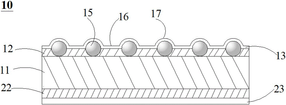
[0025] The transparent conductive film provided by the invention can be used in display terminals requiring capacitive touch panels, such as mobile phones and tablet computers.

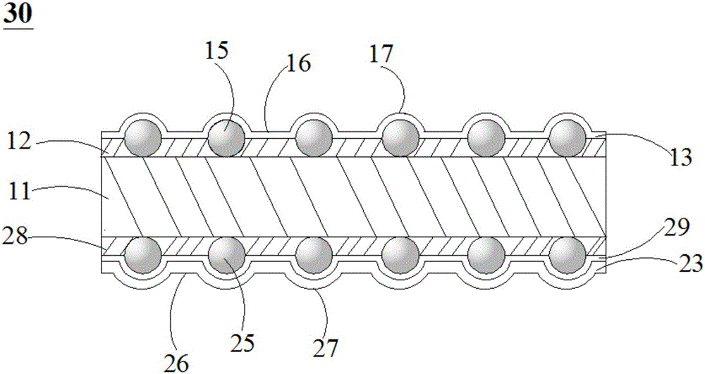
[0026] like figure 1 As shown, the transparent conductive film 10 in the first embodiment of the present invention has a substrate 11, and the substrate 11 includes a first surface (ie figure 1 The upper surface of the middle substrate 11) and the second surface (i.e. figure 1 the lower surface of the middle substrate 11). The first composite layer 12 and the first transparent conductor layer 13 are sequentially arranged on the first surface of the substrate 11 , and the second composite layer 22 and the second transparent conductor layer 23 are sequentially arranged on the second surface of the substrate 11 .

[0027] The substrate 11 may be formed by an amorphous polymer film, and the material of the film may be amorphous polycycloolefin, polycarbonate or polyimide. A first composite layer 12 con...


PUM

PropertyMeasurementUnit
thicknessaaaaaaaaaa
thicknessaaaaaaaaaa
diameteraaaaaaaaaa

Abstract

The invention relates to a transparent conductive film. The transparent conductive film has a base material, the base material includes a first surface and a second surface, and the first surface and / or the second surface of the base material is formed A composite layer of particles, and a first transparent conductor layer is formed on the first surface of the composite layer, and a second transparent conductor layer is formed on the second surface of the composite layer. By coating the composite layer of optical adjustment material and hard coating material on the surface of the amorphous polymer film substrate, it can ensure that the surface of the substrate is not easily damaged and improve the light transmittance of the conductive film. , in order to improve the visual effect of its application products and enhance the user experience; it can also solve the problem of mutual adhesion between the metal layers of adjacent transparent conductive films when the transparent conductive film is rolled into a cylindrical shape.

Description

technical field [0001] The invention relates to the technical field of conductive films, in particular to transparent conductive films used for capacitive touch panels and the like. Background technique [0002] The conductive film is composed of a substrate, a transparent conductor layer and a metal layer. In order to meet the specific requirements of electronic display devices, conductive films often need to have excellent physical properties such as high transmittance, low haze, high scratch resistance and low reflectivity. Therefore, people generally form multi-layer special functional coatings on both sides of the above-mentioned substrate, so that the conductive film has the above-mentioned excellent physical properties, thereby improving its application value. The functional coating used in the past refers to a total of four layers of hard coating and optical adjustment layer coated on the opposite surfaces of the substrate. The hard coating is used to increase the h...

Claims


Application Information

Patent Timeline
Patent Type & Authority Applications(China)
IPC IPC(8): G06F3/044H01B5/14
CPCG06F3/044H01B5/14
Inventor 王培红候晓伟李平
Owner NANCHANG O FILM DISPLAY TECH CO LTD
Why Eureka
Try Eureka