
High-power waveguide load

A high-power, waveguide technology, used in waveguide-type devices, electrical components, circuits, etc., can solve the problems of low overall assembly accuracy, affect product yield, and low processing efficiency, and ensure the stability of microwave performance and structure. The effect of low processing difficulty and improved processing efficiency

Active Publication Date: 2017-05-31
CHINA AEROSPACE TIMES ELECTRONICS CORP
View PDF3 Cites 4 Cited by
  • Summary
  • Abstract
  • Description
  • Claims
  • Application Information

AI Technical Summary

Problems solved by technology

In order to meet the demand of high power, the traditional high-power waveguide load adopts the method of processing the waveguide cavity inside the absorber to form an absorber with an integrated structure. However, because the material of the absorber is brittle in this method, it is difficult to There are problems of high processing difficulty, low processing efficiency, and high failure rate, which seriously affect the yield of products, and the accuracy of overall assembly is low

Method used


Image

  • High-power waveguide load
  • High-power waveguide load
  • High-power waveguide load

Examples


Embodiment Construction

[0027] In order to make the objectives, technical solutions and advantages of the present invention clearer, the common embodiments of the present invention will be described in further detail below with reference to the accompanying drawings.

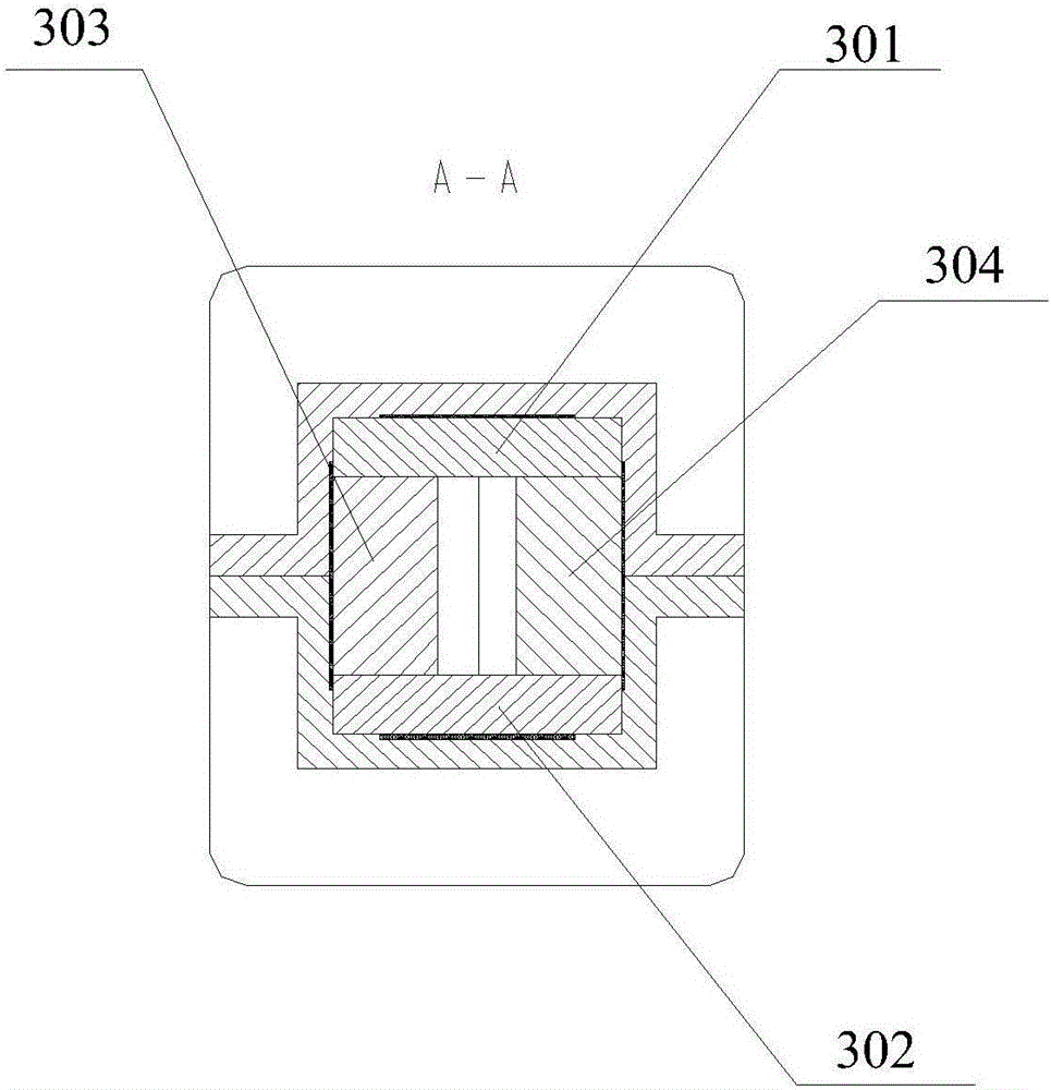
[0028] refer to figure 1 , showing a schematic diagram of the overall structure of a high-power waveguide load in an embodiment of the present invention. In this embodiment, the high-power waveguide load generally refers to a waveguide load with a power bearing capacity of hundreds of watts or even kilowatts. The high-power waveguide load may specifically include: a connecting flange 1 , a transition cavity 2 , an absorber 3 , a rear cover 4 and a heat sink 5 .

[0029] In this embodiment, the transition cavity 2 is connected with the connecting flange 1 and the heat sink 5 respectively; the rear cover plate 4 is connected with the end of the heat sink 5 away from the transition cavity 2; the absorption The body 3 is arranged in the ...


PUM


Abstract

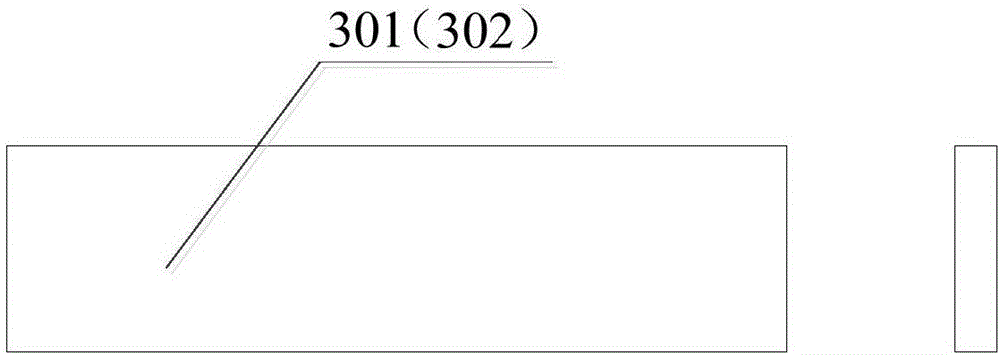
The invention discloses a high-power waveguide load comprising a connection flange, a transition cavity, an absorber, a rear cover plate, and a radiator. The transition cavity is connected with the connection flange and the radiator. The rear cover plate is connected with the end, away from the transition cavity, of the radiator. The absorber, which is arranged in the cavity of the radiator, includes a first rectangular ceramic absorbing sheet, a second rectangular ceramic absorbing sheet, a first tapered ceramic absorbing sheet, and a second tapered ceramic absorbing sheet. The sides of the first rectangular ceramic absorbing sheet, the second rectangular ceramic absorbing sheet, the first tapered ceramic absorbing sheet and the second tapered ceramic absorbing sheet are in closed connection, and the absorber obtained after connection is hollow inside. On the basis of satisfying the requirement for high power of the waveguide load, the machining difficulty of the absorber structure is reduced, and the machining efficiency and the precision of overall assembly are improved.

Description

technical field [0001] The invention belongs to the technical field of waveguide loads, and in particular relates to a high-power waveguide load. Background technique [0002] The main function of the matching load is to absorb the incident power of the microwave system as a single-port component, which is widely used in microwave technology devices. In the military aspect, it has been used more and more in the fields of radar, electronic countermeasures, satellite communication, rocket telemetry and remote control, and high-frequency testing. In terms of civilian use, it has also been widely used in mobile communications, cable television, satellite navigation, etc. The matching load can usually be divided into three types: low power, medium power and high power according to the level of withstand power. According to the different transmission lines, it can be divided into coaxial load, waveguide load and microstrip load. [0003] The basic structure of the high-power wav...

Claims


Application Information

Patent Timeline
Patent Type & Authority Applications(China)
IPC IPC(8): H01P1/26H01P1/22
CPCH01P1/22H01P1/26
Inventor 于倩蔡立兵李刚苌群峰
Owner CHINA AEROSPACE TIMES ELECTRONICS CORP
Learn More